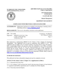
Transcription of SBOS141C - Texas Instruments
1 FEATURES 4mA TO 20mA TRANSMITTER SELECTABLE INPUT/OUTPUT RANGES:0V to +5V, 0V to +10V Inputs0mA to 20mA, 5mA to 25mA OutputsOther Ranges MAX NONLINEARITY, 14 BIT PRECISION +10V REFERENCE OUTPUT SINGLE-SUPPLY OPERATION WIDE SUPPLY RANGE: to 40 VAPPLICATIONS INDUSTRIAL PROCESS CONTROL PRESSURE/TEMPERATURE TRANSMITTERS CURRENT-MODE BRIDGE EXCITATION GROUNDED TRANSDUCER CIRCUITS CURRENT SOURCE REFERENCE FOR DATAACQUISITION PROGRAMMABLE CURRENT SOURCE FORTEST EQUIPMENT POWER PLANT/ENERGY SYSTEMMONITORINGDESCRIPTIONThe XTR110 is a precision voltage-to-current converterdesigned for analog signal transmission. It accepts inputsof 0 to 5V or 0 to 10V and can be connected for outputs of4mA to 20mA, 0mA to 20mA, 5mA to 25mA, and many othercommonly used precision on-chip metal film resistor network provides inputscaling and current offsetting.
2 An internal 10V voltage refer-ence can be used to drive external XTR110 is available in 16-pin plastic DIP, ceramic DIPand SOL-16 surface-mount packages. Commercial and in-dustrial temperature range models are +10 VReferenceVREF ForceVREF SenseVREF AdjustVIN1 (10V)VREF InVIN2 (5V)Common+VCCO ffset(zero) Adjust16mA Span4mA SpanSpan AdjustSource SenseSource ResistorGate DrivePRECISION VOLTAGE-TO-CURRENTCONVERTER/TRANSMITTERX TR110 SBOS141C JANUARY 1984 REVISED SEPTEMBER 2009 PRODUCTION DATA information is current as of publication conform to specifications per the terms of Texas Instrumentsstandard warranty. Production processing does not necessarily includetesting of all 1984-2009, Texas Instruments IncorporatedPlease be aware that an important notice concerning availability, standard warranty, and use in critical applications ofTexas Instruments semiconductor products and disclaimers thereto appears at the end of this data trademarks are the property of their respective CONFIGURATION12345678161514131211109 Source ResistorCommonVREF InVIN1 (10V)VIN2 (5V)Zero AdjustZero AdjustSpan Adjust+VCCVREF ForceGate DriveSource SenseVREF SenseVREF Adjust4mA Span16mA SpanTOP VIEWABSOLUTE MAXIMUM RATINGS(1)
3 Power Supply, + 40 VInput Voltage, VIN1, VIN2, VREF +VCCSee text regarding safe negative input voltage Temperature Range: A, B .. 55 C to +125 CK, U .. 40 C to +85 COutput Short-Circuit Duration, Gate Drive and VREF Force .. Continuous to common and +VCCO utput Current Using Internal 50 Resistor .. 40mANOTE: (1) Stresses above these ratings may cause permanent to absolute maximum conditions for extended periods may degradedevice SENSITIVITYThis integrated circuit can be damaged by ESD. Texas Instrumentsrecommends that all integrated circuits be handled with appropriateprecautions. Failure to observe proper handling and installation proce-dures can cause damage can range from subtle performance degradation tocomplete device failure.
4 Precision integrated circuits may be moresusceptible to damage because very small parametric changes couldcause the device not to meet its published CeramicJD 40 C to +85 CXTR110 BGDIP-16 CeramicJD 40 C to +85 CXTR110 KPDIP-16 PlasticN0 C to +70 CXTR110 KUSOL-16 Surface-MountDW0 C to +70 CNOTE: (1) For the most current package and ordering information, see the Package Option Addendum at the end of this document, or see the TI website at INFORMATION(1) , KP, KUXTR110 BGPARAMETERCONDITIONSMINTYPMAXMINTYPMAXU NITSTRANSMITTERT ransfer FunctionInput Range: VIN1(5)Specified Performance0+10**VVIN2 Specified Performance0+5**VCurrent, IOSpecified Performance(1)420* *mADerated Performance(1)040* *mANonlinearity16mA/20mA Span(2) of SpanOffset Current, IOSIO = 4mA(1)Initial(1) of Spanvs Temperature(1) * of Span/ Cvs Supply, VCC(1) **% of Span/VSpan ErrorIO = 20mAInitial(1) of Spanvs Temperature(1) of Span/ Cvs Supply, VCC(1) **% of Span/VOutput ResistanceFrom Drain of FET (QEXT)(3)
5 10 x 109* Input ResistanceVIN127*k VIN222*k VREF In19*k Dynamic ResponseSettling TimeTo of Span15* sTo of Span20* sSlew *mA/ sVOLTAGE REFERENCEO utput Voltage+ +10+ + *+ Temperature35501530ppm/ Cvs Supply, VCCLine **%/Vvs Output CurrentLoad **%/mAvs Time100*ppm/1k hrsTrim Range + **VOutput CurrentSpecified Performance10*mAPOWER SUPPLYI nput Voltage, VCC+ +40**VQuiescent CurrentExcluding **mATEMPERATURE RANGES pecification: AG, BG 40+85** CKP, KU0+70 COperating: AG, BG 55+125** CKP, KU 25+85 CELECTRICAL CHARACTERISTICSAt TA = +25 C and VCC = +24V and RL = 250 **, unless otherwise = 10 [(VREFIn/16) + (VIN1/4) + (VIN2/2)] /RSPAN* Specifications same as AG/KP grades.
6 ** Specifications apply to the range of RL shown in Typical Performance : (1) Including internal reference. (2) Span is the change in output current resulting from a full-scale change in input voltage. (3) Within compliance range limitedby (+VCC 2V) +VDS required for linear operation of the FET. (4) For VREF adjustment circuit see Figure 3. (5) For extended IREF drive circuit see Figure 4. (5) Unit maybe damaged. See Input Voltage Range ( C)ICC vs TEMPERATURE 4054321 200 20406080 ICC (mA) (excluding IO)IO = 20mAIO = 4mA0+VCC (V)MAXIMUM RL vs VCCRL ( )2500200015001000500203515402530IO MAX = 20mAIO MAX = 40mATYPICAL PERFORMANCE CURVESTA = +25 C, VCC = 24 VDC, RL = 250 , unless otherwise LINE REGULATION vs FREQUENCY VREF/ VCC (%/V) Ripple Frequency (Hz) POWER SUPPLY REGULATION vs FREQUENCY IO/ VCC (% of span/V) Ripple Frequency (Hz)Temperature ( C)TOTAL OUTPUT ERROR vs TEMPERATURE 40 200 20406080 Error (% of span) 2210 1 BGAGAG0 VREF Output Current (mA)(IOUT has minimal effect on TJ)
7 JUNCTION TEMPERATURE RISE vs VREF OUTPUT CURRENT Junction Temperature RiseAbove Ambient ( C)100806040202801046 VCC = +40 VVCC = +15 VVCC = +24 VMax. TJ = +175 CMax. Temp. Rise for +85 C Ambient JA = 70 PERFORMANCE CURVES (Continued)At TA = +25 C, VCC = 24 VDC, RL = 250 , unless otherwise TIME WITH POS VIN STEPVIN0V0 VIO Error( ofSpan/Box)SETTLING TIME WITH NEG VIN STEPVIN0V0 VIO Error( ofSpan/Box)PULSE RESPONSEVIN0 VIOinto500 INFORMATIONF igure 1 shows the basic connections required for 0V to 10 Vinput and 4ma to 20mA output. Other input voltage andoutput current ranges require changes in connections of pins3, 4, 5, 9 and 10 as shown in the table of Figure complete transfer function of the XTR110 is: IO =(1)RSPAN is the total impedance seen at the emitter of theinternal NPN transistor.
8 This impedance varies dependingon how pins 8, 9 and 10 are configured. Typical operatingregion configurations are shown in Figure 1. An externalRSPAN can be connected for different output current rangesas described TRANSISTORAn external pass transistor, QEXT, is required as shown inFigure 1. This transistor conducts the output signal P-channel MOSFET transistor is recommended. It must(VREF IN)16(VIN1)410 + +(VIN2)2 RSPANFIGURE 1. Basic Circuit (V) RANGE (mA)PIN 3 PIN 4 PIN 5 PIN 9 PIN 100-100-20 Com InputComComCom2-104-20 Com InputComComCom0-104-20+10V Ref InputComComOpen0-105-25+10V Ref InputComComCom0-50-20 Com ComInputComCom1-54-20 Com ComInputComCom0-54-20+10V Ref ComInputComOpen0-55-25+10V Ref ComInputComComMANUFACTURERPART (1)BVGS(1)PACKAGEF errantiZVP1304A40V20 VTO-92 ZVP1304B40V20 VTO-39 ZVP1306A60V20 VTO-92 ZVP1306B60V20 VTO-39 InternationalRectifierIRF951360V20 VTO-220 MotorolaMTP8P0880V20 VTO-220 RCARFL1P0880V20 VTO-39 RFT2P0880V20 VTO-220 SiliconixVP0300B30V40 VTO-39(preferred)
9 VP0300L30V40 VTO-92VP0300M30V 40 VTO-237VP0808B80V40 VTO-39VP0808L80V40 VTO-92VP0808M80V40 VTO-237 SupertexVP1304N240V20 VTO-220VP1304N340V20 VTO-92VP1306N260V20 VTO-220VP1306N360V20 VTO-92 NOTE: (1) BVDSS Drain-source breakdown voltage. BVGS Gate-sourcebreakdown I. Available P-Channel 16113147681091512114352R7 6250 R6 R9 50 R410k R320k R2R1R8500 +10 VReferenceZero Adjust1 F++ to 40 VSpan Adjust4mA SpanRL(250 typ)IO4 to 20mAQEXTP-ChannelMOSFET(see text)IOIO/10IO/10 VREF 0 to 10 VShortConnection(see text)+VCC16mA Span5k 15k have a voltage rating equal or greater than the maximumpower supply voltage. Various recommended types are shownin Table the supply voltage, +VCC, exceeds the gate-to-sourcebreakdown voltage of QEXT, and the output connection(drain of QEXT) is broken, QEXT could fail.
10 If the gate-to-source breakdown voltage is lower than +VCC, QEXT can beprotected with a 12V zener diode connected from gate PNP discrete transistors (Darlington-connected) can beused for QEXT see Figure 2. Note that an additional capaci-tor is required for stability. Integrated Darlington transistorsare not recommended because their internal base-emitterresistors cause excessive DISSIPATIONM aximum power dissipation of QEXT depends on the powersupply voltage and full-scale output current. Assuming thatthe load resistance is low, the power dissipated by QEXT is: PMAX = (+VCC) IFS (2)The transistor type and heat sinking must be chosen accord-ing to the maximum power dissipation to prevent overheat-ing.