Transcription of Si5341/40 Rev D Data Sheet
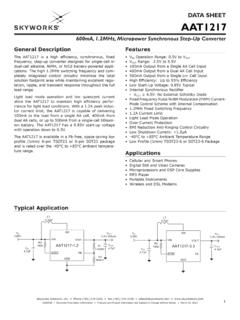
1 Si5341/40 Rev D Data SheetLow-Jitter, 10 or 4-Output, Any-Frequency, Any-Output ClockGeneratorThe any-frequency, any-output Si5341/40 clock generators combine a wide-band PLLwith proprietary MultiSynth fractional synthesizer technology to offer a versatile andhigh performance clock generator platform. This highly flexible architecture is capableof synthesizing a wide range of integer and non-integer related frequencies up to 1 GHz on 10 differential clock outputs while delivering sub-100 fs rms phase jitter per-formance with 0 ppm error. Each of the clock outputs can be assigned its own formatand output voltage enabling the Si5341/40 to replace multiple clock ICs and oscillatorswith a single device making it a true " clock tree on a chip.
2 "The Si5341/40 can be quickly and easily configured using ClockBuilderPro part numbers are automatically assigned using a ClockBuilder Pro for fast,free, and easy factory pre-programming or the Si5341/40 can be programmed via I2 Cand SPI serial : clock tree generation replacing XOs, buffers, signal format translators Any-frequency clock translation Clocking for FPGAs, processors, memory Ethernet switches/routers OTN framers/mappers/processors Test equipment and instrumentation Broadcast videoKEY FEATURES Generates any combination of outputfrequencies from any input frequency Ultra-low jitter of 90 fs rms Input frequency range: External crystal: 25 to 54 MHz Differential clock : 10 to 750 MHz LVCMOS clock : 10 to 250 MHz Output frequency range: Differential: 100 Hz to 1028 MHz LVCMOS.
3 100 Hz to 250 MHz Highly configurable outputs compatible withLVDS, LVPECL, LVCMOS, CML, and HCSL with programmable signal amplitude Si5341: 4 input, 10 output, 64-QFN 9x9 mm Si5340: 4 input, 4 output, 44-QFN 7x7 mmUp to 10 Output ClocksOUT7 OUT6 OUT5 OUT1 OUT4 OUT3 OUT2 OUT0Si5340Si5341I2C / SPIC ontrolNVMS tatus FlagsStatus Monitor4 InputClocksXBXA25-54 MHz XTALOSCM ultiSynth INT INT INT INT INT INT INT INTM ultiSynthMultiSynthMultiSynthMultiSynth INT INT INTPLL INTOUT9 OUT8 INT INTIN0IN1IN2FB_INZero DelaySkyworks Solutions, Inc. Phone [781] 376-3000 Fax [781] 376-3100 Skyworks Proprietary Information Products and Product Information are Subject to Change Without Notice November 30, 2021 11.
4 Features ListThe Si5341/40 Rev D features are listed below: Generates any combination of output frequencies from anyinput frequency Ultra-low jitter of 90 fs rms Input frequency range: External crystal: 25 to 54 MHz Differential clock : 10 to 750 MHz LVCMOS clock : 10 to 250 MHz Output frequency range: Differential: 100 Hz to 1028 MHz LVCMOS: 100 Hz to 250 MHz Highly configurable outputs compatible with LVDS, LVPECL,LVCMOS, CML, and HCSL with programmable signal ampli-tude Locks to gapped clock inputs Optional zero delay mode Glitchless on the fly output frequency changes DCO mode: as low as ppb steps Core voltage VDD: V 5% VDDA: V 5% Independent output clock supply pins V, V, or V Serial interface: I2C or SPI In-circuit programmable with non-volatile OTP memory ClockBuilder Pro software simplifies device configuration Si5341: 4 input, 10 output, 64-QFN 9x9 mm Si5340: 4 input, 4 output, 44-QFN 7x7 mm Temperature range: 40 to +85 C Pb-free, RoHS-6 compliantSi5341/40 Rev D Data Sheet Features ListSkyworks Solutions, Inc.
5 Phone [781] 376-3000 Fax [781] 376-3100 Skyworks Proprietary Information Products and Product Information are Subject to Change Without Notice November 30, 202122. Ordering GuideTable Si5341/40 Ordering GuideOrdering Part Number(OPN)Number of In-put/OutputClocksOutput clock FrequencyRange (MHz)Frequency Syn-thesis ModePackageTemperatureRangeSi5341Si5341A -D-GM1, 24 to 1028 MHzInteger andFractional64-QFN9x9 mm 40 to 85 CSi5341B-D-GM1, to 350 MHzSi5341C-D-GM1, to 1028 MHzInteger OnlySi5341D-D-GM1, to 350 MHzSi5340Si5340A-D-GM1, 24 to 1028 MHzInteger andFractional44-QFN7x7 mm 40 to 85 CSi5340B-D-GM1, to 350 MHzSi5340C-D-GM1, to 1028 MHzInteger OnlySi5340D-D-GM1, to 350 MHzSi5341/40-D-EVBSi5341-D-EVB EvaluationBoard Si5340-D-EVBNote.
6 An R at the end of the OPN to denote tape and reel ordering , factory pre-programmed devices are available. Ordering part numbers are assigned by Skyworks and the ClockBuilderPro software utility. Custom part number format is: , Si5341A-Dxxxxx-GM, where "xxxxx" is a unique numerical sequencerepresenting the preprogrammed Custom Factory Preprogrammed Devicesand Enabling Features and/or Configuration Settings Not Available inClockBuilder Pro for Factory Pre-Programmed Devices for important notes about specifying a preprogrammed device to usefeatures or device register settings not yet available in Rev D Data Sheet Ordering GuideSkyworks Solutions, Inc.
7 Phone [781] 376-3000 Fax [781] 376-3100 Skyworks Proprietary Information Products and Product Information are Subject to Change Without Notice November 30, 20213Si534fg-Rxxxxx-GMTiming product familyf = Multi-PLL clock family member (7, 6)g = Device grade (A, B, C, D)Product Revision*Custom ordering part number (OPN) sequence ID**Package, ambient temperature range (QFN, -40 C to +85 C)*See Ordering Guide table for current product revision** 5 digits; assigned by ClockBuilder ProFigure Ordering Part Number FieldsSi5341/40 Rev D Data Sheet Ordering GuideSkyworks Solutions, Inc. Phone [781] 376-3000 Fax [781] 376-3100 Skyworks Proprietary Information Products and Product Information are Subject to Change Without Notice November 30, 20214 Table of Contents1.
8 Features Ordering Functional Power-up and Frequency XA/XB clock and Crystal Input Clocks (IN0, IN1, IN2).. Input Selection (IN0, IN1, IN2, XA/XB).. Fault Status Interrupt Pin (INTRb).. Output Signal Differential Output Programmable Common Mode Voltage for Differential LVCMOS Output LVCMOS Output Impedance and Drive Strength LVCMOS Output Signal LVCMOS Output Output Output Driver State When Synchronous/Asynchronous Output Disable Zero Delay Output Digitally Controlled Oscillator (DCO) Power In-Circuit Serial Custom Factory Preprogrammed Enabling Features and/or Configuration Settings Not Available in ClockBuilder Pro for FactoryPre-Programmed Register Electrical Typical Application Detailed Block Typical Operating Pin Solutions, Inc.
9 Phone [781] 376-3000 Fax [781] 376-3100 Skyworks Proprietary Information Products and Product Information are Subject to Change Without Notice November 30, 2021510. Package Si5341 9x9 mm 64-QFN Package Si5340 7x7 mm 44-QFN Package PCB Land Top Device Revision Solutions, Inc. Phone [781] 376-3000 Fax [781] 376-3100 Skyworks Proprietary Information Products and Product Information are Subject to Change Without Notice November 30, 202163. Functional DescriptionThe Si5340/41-D combines a wide band PLL with next generation MultiSynth technology to offer the industry's most versatile and highperformance clock generator.
10 The PLL locks to either an external crystal between XA/XB or to an external clock connected to XA/XBor IN0, 1, 2. A fractional or integer multiplier takes the selected input clock or cystal frequency up to a very high frequency that isthen divided by the MultiSynth output stage to any frequency in the range of 100 Hz to 1 GHz on each output. The MultiSynth stagecan divide by both integer and fractional values. The high-resolution fractional MultiSynth dividers enable true any-frequency input toany-frequency on any of the outputs. The output drivers offer flexible output formats which are independently configurable on each ofthe outputs.