Transcription of Si5351A/B/C-B - Silicon Labs
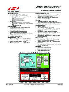
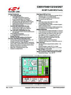
1 Si5351A/B/C-B . I 2 C - P R O G RA M M A BL E A N Y -F RE Q U E N C Y C M O S C L O C K. GENERATOR + VCXO. Features Glitchless frequency changes 10-MSOP. Generates up to 8 non-integer-related Separate voltage supply pins provide frequencies from kHz to 200 MHz level translation: I2C user definable configuration Core VDD: or V. Exact frequency synthesis at each output Output VDDO: , , or V. (0 ppm error) Excellent PSRR eliminates external Highly linear VCXO power supply filtering Optional clock input (CLKIN) Very low power consumption 20-QFN. Low output period jitter: < 70 ps pp, typ Adjustable output delay Configurable spread spectrum selectable Available in 2 packages types: at each output 10-MSOP: 3 outputs Operates from a low-cost, fixed frequency 20-QFN (4x4 mm): 8 outputs crystal: 25 or 27 MHz PCIE Gen 1 compatible Supports static phase offset Supports HCSL compatible swing Programmable rise/fall time control Ordering Information: See page 29.
2 Applications HDTV, DVD/Blu-ray, set-top box Residential gateways Audio/video equipment, gaming Networking/communication Printers, scanners, projectors Servers, storage Handheld Instrumentation XO replacement Description The Si5351 is an I2C configurable clock generator that is ideally suited for replacing crystals, crystal oscillators, VCXOs, phase-locked loops (PLLs), and fanout buffers in cost-sensitive applications. Based on a PLL/VCXO + high resolution MultiSynth fractional divider architecture, the Si5351 can generate any frequency up to 200 MHz on each of its outputs with 0 ppm error. Three versions of the Si5351 are available to meet a wide variety of applications. The si5351a generates up to 8 free-running clocks using an internal oscillator for replacing crystals and crystal oscillators. The Si5351B adds an internal VCXO and provides the flexibility to replace both free-running clocks and synchronous clocks.
3 It eliminates the need for higher cost, custom pullable crystals while providing reliable operation over a wide tuning range. The Si5351C offers the same flexibility but synchronizes to an external reference clock (CLKIN). Functional Block Diagram Si5351B (20-QFN) Si5351C (20-QFN). VDDOA VDDOA. MultiSynth MultiSynth R0 XA R0. XA CLK0 0 CLK0. PLL 0 OSC PLL. OSC A MultiSynth CLK1. MultiSynth CLK1 XB R1. XB R1 1. 1. VDDOB MultiSynth VDDOB. VCXO MultiSynth PLL R2. R2 2 CLK2. 2 CLK2 CLKIN B. VC MultiSynth CLK3. MultiSynth CLK3 R3. R3 3. 3. VDDOC VDDOC. MultiSynth MultiSynth R4 SDA R4. SDA CLK4 4 CLK4. 4. I2C SCL I2C MultiSynth CLK5. SCL MultiSynth CLK5 R5. R5 5. 5 INTR VDDOD. VDDOD MultiSynth MultiSynth R6. OEB Control R6 6 CLK6. 6 CLK6 Control Logic OEB MultiSynth CLK7. SSEN MultiSynth CLK7 Logic R7. R7 7. 7. Rev. 9/18 Copyright 2018 by Silicon Laboratories Si5351A/B/C-B .
4 Si5351A/B/C-B . Table 1. The Complete Si5350/51 Clock Generator Family Part Number I2C or Pin Frequency Reference Programmed? Outputs Datasheet si5351a -B-GT I2C XTAL only Blank 3 Si5351-B. si5351a -B-GM I2C XTAL only Blank 8 Si5351-B. Si5351B-B-GM I2C XTAL and/or Voltage Blank 8 Si5351-B. Si5351C-B-GM I2C XTAL and/or CLKIN Blank 8 Si5351-B. si5351a -Bxxxxx-GT I2C XTAL only Factory Pre-Programmed 3 Si5351-B. si5351a -Bxxxxx-GM I2C XTAL only Factory Pre-Programmed 8 Si5351-B. Si5351B-Bxxxxx-GM I2C XTAL and/or Voltage Factory Pre-Programmed 8 Si5351-B. Si5351C-Bxxxxx-GM I2C XTAL and/or CLKIN Factory Pre-Programmed 8 Si5351-B. Si5350A-Bxxxxx-GT Pin XTAL only Factory Pre-Programmed 3 Si5350A-B. Si5350A-Bxxxxx-GM Pin XTAL only Factory Pre-Programmed 8 Si5350A-B. Si5350B-Bxxxxx-GT Pin XTAL and/or Voltage Factory Pre-Programmed 3 Si5350B-B. Si5350B-Bxxxxx-GM Pin XTAL and/or Voltage Factory Pre-Programmed 8 Si5350B-B.
5 Si5350C-Bxxxxx-GT Pin XTAL and/or CLKIN Factory Pre-Programmed 3 Si5350C-B. Si5350C-Bxxxxx-GM Pin XTAL and/or CLKIN Factory Pre-Programmed 8 Si5350C-B. Notes: 1. XTAL = 25/27 MHz, Voltage = 0 to VDD, CLKIN = 10 to 100 MHz. "xxxxx" = unique custom code. 2. Create custom, factory pre-programmed parts at 2 Rev. Si5351A/B/C-B . TABLE O F C ONTENTS. Section Page 1. Electrical Specifications ..5. 2. Detailed Block Diagrams .. 10. 3. Functional Description .. 12. Input Stage .. 13. Synthesis Stages .. 14. Output Stage ..15. Spread Spectrum .. 15. Control Pins (OEB, SSEN) .. 15. 4. I2C Interface .. 16. 5. Configuring the Si5351 .. 18. Writing a Custom Configuration to RAM .. 18. Si5351 Application Examples .. 20. Replacing Crystals and Crystal Oscillators .. 20. Replacing Crystals, Crystal Oscillators, and VCXOs ..20. Replacing Crystals, Crystal Oscillators, and PLLs.
6 21. Applying a Reference Clock at XTAL Input .. 21. HCSL Compatible Outputs .. 22. 6. Design Considerations ..23. Power Supply Decoupling/Filtering .. 23. Power Supply Sequencing .. 23. External Crystal ..23. External Crystal Load Capacitors .. 23. Unused Pins ..23. Trace Characteristics .. 23. 7. Register Map Summary .. 24. 8. Register Descriptions ..24. 9. Si5351 Pin Descriptions .. 25. si5351a 20-pin QFN ..25. Si5351B 20-Pin QFN ..26. Si5351C 20-Pin QFN .. 27. si5351a 10-Pin MSOP .. 28. 10. Ordering Information .. 29. 11. Package Outlines .. 30. 20-pin QFN ..30. 12. Land Pattern: 20-Pin QFN .. 32. 10-Pin MSOP Package Outline .. 34. 13. Land Pattern: 10-Pin MSOP .. 36. 14. Top Marking ..38. 20-Pin QFN Top Marking .. 38. Top Marking Explanation .. 38. 10-Pin MSOP Top Marking .. 39. Rev. 3. Si5351A/B/C-B . Top Marking Explanation .. 39. Document Change List.
7 40. 4 Rev. Si5351A/B/C-B . 1. Electrical Specifications Table 2. Recommended Operating Conditions Parameter Symbol Test Condition Min Typ Max Unit Ambient Temperature TA 40 25 85 C. V. Core Supply Voltage VDD. V. V. Output Buffer Voltage VDDOx V. V. Notes:All minimum and maximum specifications are guaranteed and apply across the recommended operating conditions. Typical values apply at nominal supply voltages and an operating temperature of 25 C unless otherwise noted. VDD and VDDOx can be operated at independent voltages. Power supply sequencing for VDD and VDDOx requires that all VDDOx be powered up either before or at the same time as VDD. Table 3. DC Characteristics (VDD = V 10%, or V 10%, TA = 40 to 85 C). Parameter Symbol Test Condition Min Typ Max Unit Enabled 3 outputs 22 35 mA. Core Supply Current IDD. Enabled 8 outputs 27 45 mA. Output Buffer Supply Current IDDOx CL = 5 pF mA.
8 (Per Output)*. CLKIN, SDA, SCL. ICLKIN 10 A. Input Current Vin < V. IVC VC 30 A. V VDDO, default high Output Impedance ZO 50 . drive *Note: Output clocks less than or equal to 100 MHz. Rev. 5. Si5351A/B/C-B . Table 4. AC Characteristics (VDD = V 10%, or V 10%, TA = 40 to 85 C). Parameter Symbol Test Condition Min Typ Max Unit From VDD = VDDmin to valid Power-up Time TRDY output clock, CL = 5 pF, 2 10 ms fCLKn > 1 MHz From VDD = VDDmin to valid Power-up Time, PLL Bypass TBYP output clock, CL = 5 pF, 1 ms Mode fCLKn > 1 MHz From OEB pulled low to valid Output Enable Time TOE clock output, CL = 5 pF, 10 s fCLKn > 1 MHz Output Frequency Transition TFREQ fCLKn > 1 MHz 10 s Time Output Phase Offset PSTEP 333 ps/step Down spread. Selectable in %. Spread Spectrum Frequency steps. SSDEV. Deviation Center spread. Selectable in %. steps. Spread Spectrum Modulation SSMOD 30 33 kHz Rate VCXO Specifications (Si5351B only).
9 VCXO Control Voltage Range Vc 0 VDD/2 VDD V. VCXO Gain (configurable) Kv Vc = 10 90% of VDD, VDD = V 18 150 ppm/V. VCXO Control Voltage Linearity KVL Vc = 10 90% of VDD 5 +5 %. VCXO Pull Range PR VDD = V* 30 0 240 ppm (configurable). VCXO Modulation Bandwidth 10 kHz *Note: Contact Silicon Labs for V VCXO operation. Table 5. Input Clock Characteristics (VDD = V 10%, or V 10%, TA = 40 to 85 C). Parameter Symbol Test Condition Min Typ Max Unit Crystal Frequency fXTAL 25 27 MHz CLKIN Input Low Voltage VIL x VDD V. CLKIN Input High Voltage VIH x VDD V. CLKIN Frequency Range fCLKIN 10 100 MHz 6 Rev. Si5351A/B/C-B . Table 6. Output Clock Characteristics (VDD = V 10%, or V 10%, TA = 40 to 85 C). Parameter Symbol Test Condition Min Typ Max Unit Frequency Range1 FCLK 200 MHz Load Capacitance CL 15 pF. FCLK < 160 MHz, Measured 45 50 55 %. at VDD/2. Duty Cycle DC.
10 FCLK > 160 MHz, Measured 40 50 60 %. at VDD/2. tr 20% 80%, CL = 5 pF, 1 ns Rise/Fall Time tf Default high drive strength 1 ns Output High Voltage VOH VDD V. CL = 5 pF. Output Low Voltage VOL V. 20-QFN, 4 outputs running, ps, pk- 40 95. 1 per VDDO pk Period Jitter2,3 JPER. 10-MSOP or 20-QFN, ps, pk- 70 155. all outputs running pk 20-QFN, 4 outputs running, 50 90 ps, pk 1 per VDDO. 2,3. Cycle-to-Cycle Jitter JCC. 10-MSOP or 20-QFN, 70 150 ps, pk all outputs running 20-QFN, 4 outputs running, ps, pk- 50 95. 1 per VDDO pk Period Jitter VCXO2,3 JPER_VCXO. 10-MSOP or 20-QFN, ps, pk- 70 155. all outputs running pk 20-QFN, 4 outputs running, 50 90 ps, pk Cycle-to-Cycle Jitter 1 per VDDO. JCC_VCXO. VCXO2,3 10-MSOP or 20-QFN, 70 150 ps, pk all outputs running Notes: 1. Only two unique frequencies above MHz can be simultaneously output. 2. Measured over 10K cycles.