Transcription of Simulating the Avalanche Behavior of Trench Power …
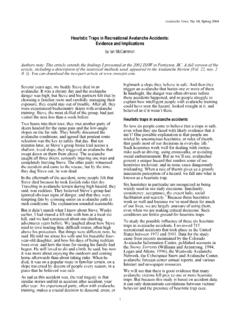
1 Simulating the Avalanche Behavior of Trench Power MOSFETs (1), (1), sch (1), (2) and (3). (1). Infineon Technologies Austria AG, Villach, Austria (2). Infineon Technologies AG, Munich, Germany (3). SEMIKRON Elektronik GmbH & Co. KG, Nuremberg, Germany Abstract The Avalanche Behavior of a new Trench Power MOSFET was investigated by means of measurement and electro-thermal simulation. Two different destruction regimes were identified experimentally: energy-related destruction and current-related destruction. Possible simulation approaches to account for the different effects are proposed. They are in good agreement with measured results. Furthermore, the experimentally found dependence on design parameters was also possible to predict qualitatively by means of simulation. Keywords: MOSFET, Trench , Avalanche Ruggedness INTRODUCTION thus making it stable to process tolerances. The drift- region doping can be increased, leading to a clearly reduced on-state resistance even below the so-called The industry's demand for devices with lower on-state silicon limit which is the on-state resistance of an resistance and good switching Behavior continues to ideal abrupt pn-junction at a given breakdown voltage exist.
2 The application fields for low-voltage devices are not limited by termination structure. for example in DC-DC Power supplies, AC-DC adapters as well as in Class-D amplifiers. In all these applications, atypical switching conditions, particularly ASPECTS OF IMPACT IONIZATION MODELS. high voltage peaks, can occur driving the device into Avalanche mode. The aim of this work is to predict, by means of numerical simulations, the maximum Mobile charges (electrons, holes) are accelerated in the Avalanche current Ias the transistor is able to sustain. As presence of an electric field thus gaining kinetic energy. well known, this current strongly depends on the load These carriers suffer collisions with the lattice and inductance Lload and decreases with increasing transfer energy to the lattice. If the transferred energy is inductance. The on-state resistance and Ias are inversely higher than a certain threshold (at least the bandgap proportional to each other thus a trade-off exists.)
3 To energy) an electron hole pair (EHP) is generated. simulate this trade-off for different cell design This process of impact ionization can be regarded as parameter variations significantly accelerates the inverse Auger effect [2]. Analytical considerations development process and the finding of a desired optimum. 200. Simulation - Chy noweth DEVICE CONCEPT 190 Simulation - Valdinoci M easurement 180. 170. BVDSS [V]. To meet the requirements aforementioned the principle of charge balancing by means of field plates is 160. employed in the new OptiMOS 2-family [1]. In contrast to standard Trench MOS structures that exhibit a linearly 150. decreasing electric field with a maximum at the 140. body/drift region pn-junction, the electric field distribution employing the field plate principle is almost 130. constant. A deep Trench penetrates the whole drift 120. region. A highly conductive region (field plate). insulated from the drift region provides mobile charges 0 100 200 300.
4 To balance the drift region donors under blocking T [ C]. conditions. The blocking capability is mainly : Measurement of BVDSS as function of temperature determined by the insulator thickness at the Trench compared to simulated values obtained with impact ionization bottom and not by the doping density in the drift region models of Chynoweth and Valdinoci, respectively showed an inversely proportional dependence of ionization rate to electric field [2]: (. ~ exp 1 / E x ) (1). with x = 1 at low electric fields and x = 2 at relatively high electric fields [3]. Avalanche breakdown occurs if the so-called ionization integral approaches 1. Several models have been developed to account for this effect in numerical simulations, for example [4,5,6]. The widely used Chynoweth model [5] with the parameters obtained by van Overstraeten and de Man [7] was compared to the recently proposed model by Valdinoci [8] and to experimental results.
5 Measurements performed on manufactured devices revealed a temperature coefficient (TC) of breakdown voltage of ~ /K. As depicted in Fig. 1, Valdinoci's Fig. 3: Measurement of energy-related destruction. The fast model delivers better temperature dependence than decay of VDRAIN indicates destruction. Chynoweth's model compared to measurement, with temperature coefficients of ~ /K and ~ /K, respectively. current Ias on load inductance in the circuit. MEASUREMENT SETUP DESTRUCTION MECHANISMS. In certain applications a failure mode called unclamped The first mechanism is related to the heat dissipation inductive switching (UIS) can occur. The aim of the capability of the device and thus will be called energy- UIS test is to determine the maximum Avalanche current related destruction. A typical example is shown in the device is able to sustain. Fig. 2 shows the circuit Fig. 3. used for the measurements and simulations. After the gate is turned off, the current cannot change It consists of a voltage source, an external switch, a instantaneously.
6 To maintain the current, the device is freewheeling diode, an inductance and the device under driven into breakdown and the current decreases at a test ( ). While the transistor is turned on rate: (VGS = 20V) and the external switch is closed, the di VDS VD. current ramps up according mainly to the inductance = (2). dt L. and the applied voltage. After turning off the device (and at the same time disconnecting the voltage source), Due to the presence of a high electric field and high the energy stored in the inductance must be dissipated in current density, the lattice temperature increases, as the transistor. Since the current continues to flow described by the heating term: through the inductance the transistor is forced to Pth r r maintain the current. Thus it is driven into Avalanche = E J (3). V. mode. The ramping process is iterated for a higher current until The breakdown voltage Vbr rises due to increased the device fails.
7 By repeating this process with different carrier-phonon interaction caused by the increase in inductances the UIS Behavior can be well characterized, temperature, Vbr exhibits a positive temperature in particular the dependence of maximum Avalanche coefficient. This supports a homogenous current distribution since no filament is expected to build up. The temperature continues to rise until it gets in the vicinity of the so-called intrinsic temperature Tint. It is defined as the temperature at which intrinsic carrier concentration ni(T) equals background doping ND and can empirically found to be [10]: 3. 7000K . n i (T ) = 1016 T 2 exp cm 3. (4). T . At this point, the device is not able to dissipate more energy thus if the current continues it will be destructed due to intrinsic conduction effects induced by too high a Fig. 2: Principle circuit to determine the unclamped inductive temperature. Of course, this value serves only as an switching Behavior of a transistor.
8 The voltage source is upper limit. The intrinsic conduction sets in at a disconnected when the transistor turns off. somewhat lower temperature thus the intrsinsic T=25 C. T=175 C. ID [A/um]. Isnap 0 25 50 75 100 125 150 175. VDS [V]. Fig. 6: Measurement of current-related destruction. The short Fig. 4: Simulated breakdown curves for two different time to destruction is apparent. temperatures temperature Tint can only be regarded as a soft limit. Tint transistor. The holes generated by impact ionization can also be extracted by measuring the Avalanche flow through the p-body region of the n-channel current Ias at different temperatures and for various MOSFET thus creating a potential drop in the base inductances. All curves, if extrapolated, intersect the region of the parasitic bipolar transistor. If this potential abscissa at the same point, this point being the intrinsic drop exceeds the built-in potential of the base-emitter temperature for this particular technology Fig.
9 5 shows diode the parasitic BJT will turn-on, latch-up. Since measured values and their respective extrapolation for a BJT has a negative temperature coefficient of the new Trench technology (OptiMOS 2) and the planar breakdown voltage latch-up is self-amplifying, thus the predecessor technology (SIPMOS ) [1]. The Trench current concentrates on a small region of the device. technology exhibits a higher Tint due to a higher doping Fig. 6. depicts a current-related destruction Behavior of of the epitaxial layer. A narrow distribution of the a device. The short transient time (<<1 s) until the Avalanche current Ias over a large number of devices is device is destroyed indicates a different mode than characteristic for this mechanism. energy-related destruction. A rather broad distribution The second mechanism that results in the destruction of of measured Ias over large number of devices is MOSFET devices is called current-related destruction characteristic for this mechanism.
10 Since it typically occurs at higher current densities. It is The breakdown characteristics for two different caused by the turn-on (latch-up) of the parasitic npn- temperatures can be seen in Fig. 4. A region with negative differential resistance (NDR) does exist and causes the voltage to decrease. This snapback effect is related to the second breakdown of the MOSFET. The Ias 3/2 [A 3/2. ] Ias [A]. current at which this snapback occurs shall be defined 2000. as snapback current Isnap. It does not only depend on the Op tiM OS-2 Sip M OS 150. 1800 temperature but also on cell design as was determined experimentally and outlined in the next section. 1600 Furthermore, the voltage starts to increase again thus 1400 1mH 1mH confining the region of NDR to certain current values. 125. 3mH 3mH. 1200. 1000 100 EXPERIMENTAL RESULTS. 800. 600 75. Three different device types A, B and C were used to 400 investigate the influence of structural variations on 50.