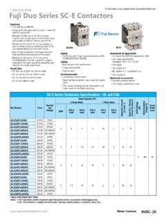
Transcription of Small Signal Zener Diodes - Vishay Intertechnology
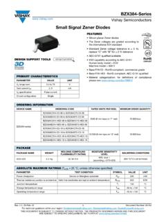
1 Semiconductors Rev. , 13-Feb-181 Document Number: 85763 For technical questions within your region: DOCUMENT IS SUBJECT TO CHANGE WITHOUT NOTICE. THE PRODUCTS DESCRIBED HEREIN AND THIS DOCUMENTARE SUBJECT TO SPECIFIC DISCLAIMERS, SET FORTH AT Signal Zener DiodesDESIGN SUPPORT TOOLSFEATURES Silicon planar Zener Diodes The Zener voltages are graded according to the international E24 standard. Standard Zener voltage tolerance is 5 %, indicated by the C in the ordering code. Replace C with B for 2 % tolerance. AEC-Q101 qualified available ESD capability acc. to AEC-Q101: human body model: > 8 kV, machine model: > 800 V Base P/N-E3 - RoHS-compliant, commercial grade Base P/N-HE3 - RoHS-compliant, AEC-Q101 qualified Material categorization: for definitions of compliance please see CHARACTERISTICSPARAMETERVALUEUNITVZ range to 75 VTest current IZT2; 5mAVZ specificationPulse currentCircuit configurationSingle20421123click logo to get startedAvailableModelsAvailableORDERING INFORMATIONDEVICE NAMEORDERING CODETAPED UNITS PER REELMINIMUM ORDER QUANTITYBZX84-seriesBZX84C2V4-E3-08 to BZX84C75-E3-083000 (8 mm tape on 7" reel)15 000 BZX84B2V4-E3-08 to BZX84B75-E3-08 BZX84C2V4-HE3-08 to BZX84C75-HE3-08 BZX84B2V4-HE3-08 to BZX84B75-HE3-08 BZX84C2V4-E3-18 to BZX84C75-E3-1810 000 (8 mm tape on 13" reel)10 000 BZX84B2V4-E3-18 to BZX84B75-E3-18 BZX84C2V4-HE3-18 to BZX84C75-HE3-18 BZX84B2V4-HE3-18 to BZX84B75-HE3-18 PACKAGEPACKAGE NAMEWEIGHTMOLDING COMPOUND FLAMMABILITY RATINGMOISTURE SENSITIVITY LEVELSOLDERING mgUL 94 V-0 MSL level 1(according J-STD-020)260 C/10 s at terminalsABSOLUTE MAXIMUM RATINGSPARAMETERTEST CONDITIONSYMBOLVALUEUNITP ower dissipationTamb = 25 C, device on fiberglass substrate, acc.
2 Layout on page 7 Ptot300mWThermal resistance junction to ambient airTamb = 25 C, device on fiberglass substrate, acc. layout on page 7 RthJA420K/WJunction temperatureTj150 CStorage temperature rangeTstg-65 to +150 COperating temperature rangeTop-55 to +150 Semiconductors Rev. , 13-Feb-182 Document Number: 85763 For technical questions within your region: DOCUMENT IS SUBJECT TO CHANGE WITHOUT NOTICE. THE PRODUCTS DESCRIBED HEREIN AND THIS DOCUMENTARE SUBJECT TO SPECIFIC DISCLAIMERS, SET FORTH AT CHARACTERISTICS (Tamb = 25 C, unless otherwise specified)PART NUMBERMARKING CODEZENER VOLTAGE RANGETEST CURRENTREVERSE LEAKAGE CURRENTDYNAMIC RESISTANCEf = 1 kHzTEMPERATURE COEFFICIENTVZ at IZT1 IZT1 IZT2IR at VRZZ at IZT1 ZZK at IZT2 VZ at IZT1 VmA AV 10-4/ Semiconductors Rev. , 13-Feb-183 Document Number: 85763 For technical questions within your region: DOCUMENT IS SUBJECT TO CHANGE WITHOUT NOTICE.
3 THE PRODUCTS DESCRIBED HEREIN AND THIS DOCUMENTARE SUBJECT TO SPECIFIC DISCLAIMERS, SET FORTH AT CHARACTERISTICS (Tamb = 25 C, unless otherwise specified)PART NUMBERMARKING CODEZENER VOLTAGE RANGETEST CURRENTREVERSE LEAKAGE CURRENTDYNAMIC RESISTANCEf = 1 kHzTEMPERATURE COEFFICIENTVZ at IZT1 IZT1 IZT2IR at VRZZ at IZT1 ZZK at IZT2 VZ at IZT1 VmA AV 10-4/ Semiconductors Rev. , 13-Feb-184 Document Number: 85763 For technical questions within your region: DOCUMENT IS SUBJECT TO CHANGE WITHOUT NOTICE. THE PRODUCTS DESCRIBED HEREIN AND THIS DOCUMENTARE SUBJECT TO SPECIFIC DISCLAIMERS, SET FORTH AT CHARACTERISTICS (Tamb = 25 C, unless otherwise specified)Fig. 1 - Forward CharacteristicsFig. 2 - Admissible Power Dissipation vs. Ambient TemperatureFig. 3 - Dynamic Resistance vs. Zener CurrentFig. 4 - Dynamic Resistance vs. Zener CurrentFig. 5 - Dynamic Resistance vs. Zener CurrentFig. 6 - Thermal Differential Resistance vs.
4 Zener = 100 CTJ = 25 C18115mW4001000300200 PtotTamb0100200 = 25 mA TJ = 25 = 25 C47 + 5143393610218121103543254321021 Rzth543210 12345234510100 VVZ at IZ = 5 mAnegativepositive VZTjRzth = RthA x VZ x Semiconductors Rev. , 13-Feb-185 Document Number: 85763 For technical questions within your region: DOCUMENT IS SUBJECT TO CHANGE WITHOUT NOTICE. THE PRODUCTS DESCRIBED HEREIN AND THIS DOCUMENTARE SUBJECT TO SPECIFIC DISCLAIMERS, SET FORTH AT 7 - Dynamic Resistance vs. Zener VoltageFig. 8 - Temperature Dependence of Zener Voltage VoltageFig. 9 - Change of Zener Voltage vs. Junction TemperatureFig. 10 - Temperature Dependence of Zener Voltage VoltageFig. 11 - Change of Zener Voltage vs. Junction TemperatureFig. 12 - Change of Zener Voltage from Turn-on up to the Point of Thermal Equilibrium vs. Zener Voltage1812210075432754321 Rzj10Tj = 25 CIZ = 5 mA12345234510100 VVZ18123 2520151050- 5mV/ C VZTj12345234510100 VVZ5 mA1 mA20 mAIZ =18124VZ at IZ = 5 - 1- 120 140 C 18125 100806040200mV/ C VZTj020408060100 VVZIZ = 5 mA18126 97531- 1 VVZ86420010060Tj204012080140 CIZ = 2 mA51433618127 - VVZ at IZ = 5 mAVZ = Rzth x IZ Semiconductors Rev.
5 , 13-Feb-186 Document Number: 85763 For technical questions within your region: DOCUMENT IS SUBJECT TO CHANGE WITHOUT NOTICE. THE PRODUCTS DESCRIBED HEREIN AND THIS DOCUMENTARE SUBJECT TO SPECIFIC DISCLAIMERS, SET FORTH AT 13 - Change of Zener Voltage from Turn-on up to the Point of Thermal Equilibrium vs. Zener VoltageFig. 14 - Breakdown CharacteristicsFig. 15 - Breakdown CharacteristicsFig. 16 - Breakdown Characteristics18128 543210 VVZ020406080100 VVZIZ = 5 mAIZ = 2 mAVZ = Rzth x IZ 18111 Test current IZ 5 mA123456789010 = 25 VVZmA3020100lZ33 Test current IZ 5 mATj = 25 C1012151822273618113mA1086420lZ1020 30 40 50 60 70 80 900100 VVZ4339 Test current IZ 5 mATj = 25 Semiconductors Rev. , 13-Feb-187 Document Number: 85763 For technical questions within your region: DOCUMENT IS SUBJECT TO CHANGE WITHOUT NOTICE. THE PRODUCTS DESCRIBED HEREIN AND THIS DOCUMENTARE SUBJECT TO SPECIFIC DISCLAIMERS, SET FORTH AT FOR RthJA TESTT hickness: fiberglass " ( mm) Copper leads " ( mm)PACKAGE DIMENSIONS in millimeters (inches): SOT-231745115 ( )12 ( ) ( )5 ( ) ( )3 ( )1 ( )1 ( )2 ( )2 ( ) ( ) ( )Foot print recommendation:Rev.
6 8 - Date: 23. Sep. 200917418 Document no.: ( )1 ( ) ( )1 ( ) ( ) ( ) ( ) ( ) ( ) ( ) ( ) ( ) ( ) ( ) ( ) ( ) ( ) ( ) ( ) ( ) ( ) ( ) ( )2 ( ) ( ) ( )0 to 8 ( ) ( ) ( ) ref. ( ref.)Legal Disclaimer Revision: 08-Feb-171 Document Number: 91000 Disclaimer ALL PRODUCT, PRODUCT SPECIFICATIONS AND DATA ARE SUBJECT TO CHANGE WITHOUT NOTICE TO IMPROVE RELIABILITY, FUNCTION OR DESIGN OR OTHERWISE. Vishay Intertechnology , Inc., its affiliates, agents, and employees, and all persons acting on its or their behalf (collectively, Vishay ), disclaim any and all liability for any errors, inaccuracies or incompleteness contained in any datasheet or in any other disclosure relating to any makes no warranty, representation or guarantee regarding the suitability of the products for any particular purpose or the continuing production of any product. To the maximum extent permitted by applicable law, Vishay disclaims (i) any and all liability arising out of the application or use of any product, (ii) any and all liability, including without limitation special, consequential or incidental damages, and (iii) any and all implied warranties, including warranties of fitness for particular purpose, non-infringement and merchantability.
7 Statements regarding the suitability of products for certain types of applications are based on Vishay s knowledge of typical requirements that are often placed on Vishay products in generic applications. Such statements are not binding statements about the suitability of products for a particular application. It is the customer s responsibility to validate that a particular product with the properties described in the product specification is suitable for use in a particular application. Parameters provided in datasheets and / or specifications may vary in different applications and performance may vary over time. All operating parameters, including typical parameters, must be validated for each customer application by the customer s technical experts. Product specifications do not expand or otherwise modify Vishay s terms and conditions of purchase, including but not limited to the warranty expressed as expressly indicated in writing, Vishay products are not designed for use in medical, life-saving, or life-sustaining applications or for any other application in which the failure of the Vishay product could result in personal injury or death.
8 Customers using or selling Vishay products not expressly indicated for use in such applications do so at their own risk. Please contact authorized Vishay personnel to obtain written terms and conditions regarding products designed for such license, express or implied, by estoppel or otherwise, to any intellectual property rights is granted by this document or by any conduct of Vishay . Product names and markings noted herein may be trademarks of their respective owners. 2017 Vishay Intertechnology , INC. ALL RIGHTS RESERVED