Transcription of Stackup Planning Pt1 PCBD-June2015 - iCD
1 48 4HE 0#" -AGAZINE s /CTOBER differential Pair Routingby Barry Olney IN-CIRCUIT DESIGN PTY LTD, AUSTRALIAS U M M A R YBEYOND DESIGNC O L U M NA differential pair is two complementary transmission lines that transfer equal and opposite signals down their length. The debate rages as some argue that since the two halves of the pair carry equal and opposite signals, a good ground connection is not required as the return current flows in the opposite signal. In addition, tight coupling between the signals is better than loose coupling, as it reduces undesirable coupling from aggressor say that beyond the fact that differential pairs transfer equal and opposite signals, there are no special requirements that need to be considered when using differential pairs.
2 They should be treated as two single-ended signals. The signals of a differential pair don t need to be routed together, should not be tightly coupled and are not required to be routed to the differential am not getting into this argument, as I look at PCB design from a practical designer s point of view, the theory can be left to the experts to , most agree on the advantages of differential signaling: 1. The ground (reference) connection between the driver and load can be poor and the signal quality will not be The signal can be attenuated significantly (20 dB) and still function properly. 3. Because of the high noise immunity, they can carry extremely high data rates (10 Gb/s) compared to single-ended transmission The equal and opposite nature of the differential pair means that demand on the power distribution network is less than for a similar single-ended data both points of view in mind, I consider that symmetry is the key to successfully deploying differential signals in high-speed designs.
3 Maintaining the equal and opposite amplitude and timing relationship is the principal concept when using differential pairs also require matched length traces. For instance, DDR2 clocks need to be matched to within 25 MIL. This ensures that there is no skew between the signals of the pair, and flight times will be identical, which is an important factor. To control crosstalk, keep aggressor signals as far away as possible from differential pairs, especially in Microstrip (outer layers). A good rule of thumb: Clearance = 3 x trace width. Additionally, reducing the signal layer to reference plane spacing (dielectric) improves the routing is dense then consider setting the clearance design rules to 2 x trace width to start. There is a good feature in Altium Designer that I use frequently: the Parallel Segment rule.
4 This enables you to set a gap of 4 MIL (on the same layer or adjacent layer) for a maximum length of 500 MIL; then, the spacing must increase to 8 application note discusses the selection and optimal settings of differential pair design rules. When it comes to successfully deploying differential signals in high-speed designs, symmetry is the key. Maintaining the equal and opposite amplitude and timing relationship is the principal concept when using differential 4HE 0#" -AGAZINE s /CTOBER In addition, placing copper pours next to one side of a pair isolates the two halves of the pair. This is another good reason not to pour copper ground planes on high-speed digital designs. Keep ground pours well away from differential pairs.
5 If you must have them use a clearance of 3 x trace amount of real estate available is also to be considered. Typically, a DDR2 board will be routed with 4-MIL trace and 4-MIL clearance with vias 20-MIL pad and 8-MIL hole. This allows us to place the fanout vias under the BGA device and route out to open space. Generally, the 100-ohm differential clock will start at 4/4 (trace/clearance) and once clear of the BGA revert to 4/8. Figure 2 below shows a DDR2 clock routed differentially from the processor with a 4-MIL trace and 8-MIL spacing. The signals come out of the BGA, fanout within 200 MIL and drop to an internal signal layer, and are then distributed to the memory this case, I was fortunate not to have an obstacle in the path of this pair.
6 It is typical however to have to split the pair around a via, pin or other obstacle to get to the load. This is where tightly coupled pairs come unstuck. That is, the gap, and hence, differential impedance cannot be maintained and the result is a much higher impedance in the diverted area, which creates brings us to another controversial point: whether to have close (tight) or loose coupling of the differential signals (where tight coupling is defined as 4/4; loose coupling is 4/12). Tight coupling is good for densely routed boards (aren t they all), but with tight coupling the clearance must be maintained along the entire length of the signal. As mention previously, this is not always possible because of the inevitable obstacle.
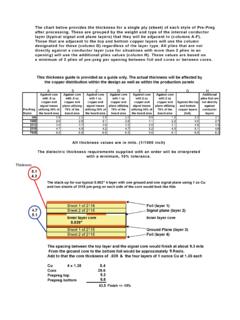
7 Leaving the theory of differential signaling aside, here s what works:The rule of thumb: Gap = 2 x trace width. Therefore, for a 4-MIL trace a gap or clearance (edge to edge) should be in the order of 8 MIL. If we expand the 8-MIL gap to 28 MIL around an obstacle ( , 20-MIL via) the differential impedance increases by ohms ( ), but if we start with tight coupling of 4/4 and increase to 4/28 around an obstacle then the impedance does a massive jump of 25 ohms (25%). Clearly, this is way over the acceptable +/- 10% for controlled impedance boards (not considering the fabrication process variables).Figure 1: Parallel Segment 2: DDR2 clock at 4-MIL trace 8-MIL 3: The gap increased from 8 MIL to 28 MIL around an obstacle then back to 8 PAIR ROUTING continues/CTOBER s 4HE 0#" -AGAZINE 51 The above Stackup was built with the ICD Stackup Planner (download from ).
8 The new HDI Designer Edition includes multiple differential pair definitions per days it is quite common to have differential DDR2 clocks, USB pairs, PCI express pairs, etc., sharing the same layers on HDI boards. Until now, the designer had to calculate each impedance separately and somehow display the results meaningfully to fellow designers and the PCB fabricator. It is usually difficult enough to calculate one differential impedance, but the designer must now run both 100-ohm and 90-ohm impedances on the same PAIR ROUTING continuesTrace Width (MIL) Clearance (MIL) Zdiff (ohms) % increase 4 8 4 28 ideal4 4 4 28 25% out of toleranceFigure 4: DDR2 clock differential pair of 100-ohms 5: Graph of trace width vs.
9 Clearance for 100-ohm and 90-ohm differential 4HE 0#" -AGAZINE s /CTOBER As previously mentioned, the 4/8 differential pair works well for 100-ohm differential impedance on this particular substrate. However, the 90-ohm USB signal would be best routed at , as any increase in trace separation will have minimal effect on new HDI Designer Edition of the ICD Stackup Planner addresses these issues. Simply select the desired number of layers 2 to 16 (or create your own unlimited layer Stackup ) and start inserting differential pairs. As you insert a new differential pair, the ICD Stackup Planner automatically calculates both the single-ended (characteristic) and differential impedance of each layer. Simply adjust the variables to achieve the desired impedance of 100 or 90 ohms for a common Conclusion1.
10 Symmetry is the key to successfully deploying differential signals in high-speed designs. Maintaining the equal and opposite amplitude and timing relationship is the principal concept when using differential pairs. 2. Match the length of each signal of the pair. This ensures that there is no skew between the signals of the pair, and flight times will be Route the differential pairs to impedance and at the optimal spacing: Gap = 2 x trace To control crosstalk, keep aggressors far away from differential pairs, especially on Microstrip (outer layers). A good rule of thumb here is Gap = 3 x trace width. PCBR eferences !DVANCED $ESIGN FOR 3-4 n "ARRY /LNEY2. Design Techniques for DDR, DDR2 & $$2 n "ARRY /LNEY %MBEDDED 3 IGNAL 2 OUTING n "ARRY /LNEY #OPPER 'ROUND 0 OURS n "ARRY /LNEY 0 RACTICAL $IFFERENTIAL 0 AIR $ESIGN n %RIC Bogatin6.