Stackup
Found 9 free book(s)
High Speed USB Platform Design Guidelines - USB.org
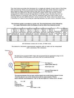
www.usb.orgHigh Speed USB Platform Design Guidelines Page 7 4/26/01 Figure 3 Recommended trace spacing (mils) for the stackup given in Section 3.7 3.3 High Speed USB Termination

TWL1200 PCB Design Guidelines - Texas Instruments
www.ti.com1 Overview 2 Layout and Design Guidelines 2.1 Layer Stackup Overview www.ti.com This document provides helpful guidelines that should be followed during TWL1200 …

Stackup Planning Pt1 PCBD-June2015 - iCD
www.icd.com.au 51 The above stackup was built with the ICD Stackup Planner (download from www. icd.com.au). The new HDI Designer Edition includes multiple differential pair …

AN 18.6 - SMSC Ethernet Physical Layer Layout …
ww1.microchip.comSMSC Ethernet Physical Layer Layout Guidelines SMSC AN18.6 5 Revision 0.8 (10-27-08) APPLICATION NOTE Figure 2.5 Common Mode Choke on PCB DC Input
Prepreg thickness chart - Advanced Circuits
www.4pcb.comPrepreg Signal Ground Foil Signal Ground Foil Signal Ground Foil 106 1.8 1.9 2.0 1.7 1.8 1.9 1.5 1.6 1.7 1080 2.4 2.6 2.8 2.3 2.5 2.8 2.1 2.3 …

2012 Seminar Series Announcement
www.advanceddimensionalmanagement.comA 2 1 3 2 . 6 - 0 . 2 0 6 2 7 5 1 . 6 1 . 4 4 + 0 . 2 7 . 5 - 0 . 8 A d v a n c e d 8D i m e n s i o n a l M a n a g e m e n t 2 1 5 0 S W T r u m p e t r D r v e S h e r w

PCB Layout Checklist - eTech-WEB
www.etech-web.comPCB Layout Checklist To start quoting a PCB layout, you can send the following information in an email to sales@ etech-web.com. A netlist in a suitable format.

Digital Signals Integrity Tutorial - Sonnet Software
www.sonnetsoftware.comDigital Signals Integrity Tutorial Sonnet Microstrip Models Thanks to Sonnet’s Application Engineer, Greg Kinnetz and the TCNJ Spring 2014 ELC 441 Digital Engineering Systems Class,
Understanding TI?s PCB Routing Rule-Based DDR …
www.ti.com1 Classical High-Speed Design Flow Application Report SPRAAV0A–July 2008 Understanding TI’s PCB Routing Rule-Based DDR Timing Specification …
Similar queries
Stackup, TWL1200, Texas Instruments, Differential, SMSC Ethernet Physical Layer Layout, SMSC Ethernet Physical Layer Layout Guidelines, Prepreg thickness chart, Announcement, PCB Layout Checklist, Digital Signals Integrity Tutorial, Routing Rule-Based DDR, Routing Rule-Based DDR Timing Specification