Transcription of TPS6123x High Efficiency Synchronous Step Up …
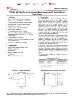
1 (%) Iout (A) Vin = VVin = VVin = VC008 Vout = V TPS61230 VINVOUTFBVINGNDENSWPGC23x22 HC122 &BuyTechnicalDocumentsTools &SoftwareSupport &CommunityTPS61230,TPS61231,TPS61232 SLVSAQ2C JANUARY2014 REVISEDOCTOBER2014 TPS6123xHigh EfficiencySynchronousStep Up Converterswith 5-A Switches1 Features3 DescriptionTheTPS6123xdevicefamilyis a highefficiency1 V to Vsynchronousstepup converterwith compactsolution V to is optimizedfor productspoweredby a one- Up to 96%EfficiencySynchronousBoostcell Li-Ionbattery,or a regulatedpowerrail of integratesa 5-A switchandis capableofdeliveringoutputcurrentsup to A at a 5-V output 5-V PowerConversionwith a deviceis basedon aCurrentquasi-constanton-timevalleycurre ntmodecontrol InputSupplyVoltageSupervisorwith typicaloperatingfrequencyis 2 MHz,Threshold/Hysteresiswhichallowstheus eof smallinductorsand PowerSaveModefor LightLoadEfficiencycapacitorsto achievea adjustable LoadDisconnectDuringShutdownoutputvoltag evia an externalresistordivider,and the OutputOverVoltageProtectionTPS61232provi desa fixedoutputvoltageof 5 V.
2 ProgrammableSoft StartDuringlight loads,the TPS6123xautomaticallyenters PowerGoodOutputpowersavemodefor maximumefficiencyat lowest shutdown,theloadiscompletelydisconnected fromthe input,and the input OutputCapacitorDischarge(TPS61231)curren tconsumptionis reducedto A 3 mm x 3 mm x mm VSONP ackagedeviceintegratesa wellas the2 Applicationshysteresisof the enablecomparatorare adjustablewithexternalresistorsandsuppor tapplication Low VoltageLi-IonBatteryPoweredProductsspeci ficsystempowerup anddownrequirements. USBP owerSupplyOtherfeatureslike outputovervoltageprotection, TabletPCsthermalshutdownprotection,anda powergoodoutputare built-in. PowerBanks,BatteryBackupUnits IndustrialMeteringEquipmentsThe devicesare availablein a 3 mm x 3 mm x (1)PARTNUMBERPACKAGEBODYSIZE(NOM)TPS6123 0 TPS61231(2)VSON(10) x (1) For all availablepackages,see the orderableaddendumatthe end of the datasheet.
3 (2) factoryfor moreinformationTPS61230 TypicalApplicationTPS61230 TypicalApplicationEfficiency1An IMPORTANTNOTICEat the end of this datasheetaddressesavailability,warranty, changes,use in safety-criticalapplications,intellectual propertymattersand ,this ,TPS61231,TPS61232 SLVSAQ2C JANUARY2014 Applicationsand Pin Configurationand Deviceand Mechanical,Packaging,and RevisionHistoryChangesfromRevisionB (June2014)to RevisionCPage ChangedElectricalCharacteristicsin the IQrow; VOUT= V to VOUT= No (March2014)to RevisionBPage AddedTPS61232to the Changedthe Changedthe Changedthe (September2013)to RevisionAPage DeletedTPS61232fromthe Changedthe datasheetto the new TI Changedthe DescriptionFrom:inputcurrentconsumptioni s reducedto A typicalTo: inputcurrentconsumptionis reducedto A Changedthe.
4 8 Deletedthe ProgrammingThe ChangedFigure14 labelFrom:Startup(A) To: Startup( )..152 SubmitDocumentationFeedbackCopyright 2014,TexasInstrumentsIncorporatedProduct FolderLinks:TPS61230 TPS61231 TPS61232 GNDVOUTVOUTPGSWSWVINENHYSFBSS12345109876 11 TPS61230,TPS61231, JANUARY2014 REVISEDOCTOBER20145 DeviceComparisonTablePARTNUMBEROUTPUTVOL TAGEOUTPUTDISCHARGETPS61230 DRCA djustableNoTPS61231 DRC(1)AdjustableYesTPS61232 DRC5-V fixedoutputNo(1) factoryfor moreinformation6 Pin Configurationand Functions11-PINVSONDRCPACKAGE(TopView)Pi n FunctionsPINI/ODESCRIPTIONNAMENUMBERSW1, 2 PWRThe switchpin of the is connectedto the drainof the , be left floatingif not startuppin. A soft startupcapacitorconnectsto this pin to set the soft connectedto VOUTon hysteresisprogrampin.
5 See the applicationsectionfor be left floatingif not deviceand turnsit pin mustbe 2014,TexasInstrumentsIncorporatedSubmitD ocumentationFeedback3 ProductFolderLinks:TPS61230 TPS61231 TPS61232 TPS61230,TPS61231,TPS61232 SLVSAQ2C JANUARY2014 (unlessotherwisenoted)(1)MINMAXUNITV oltagerangeat pins(2)EN, FB, PG, SS, HYS,VIN,VOUT,SW ,TJ 40150 C(1)Stressesbeyondthoselistedunderabsolu temaximumratingsmay causepermanentdamageto the stressratingsonly,and functionaloperationof the deviceat theseor any otherconditionsbeyondthoseindicatedunder recommendedoperatingconditionsis not absolute-maximum-ratedconditionsfor extendedperiodsmy affectdevicereliability.(2)All voltagesare with respectto CHumanbodymodel(HBM),per ANSI/ESDA/JEDECJS-001,all pins(1) 22kVElectrostaticVESDC hargeddevicemodel(CDM),per JEDEC specificationJESD22-C101,allVdischarge 500500pins(2)(1)JEDEC documentJEP155statesthat 500-VHBM allowssafe manufacturingwith a standardESDcontrolprocess.
6 (2)JEDEC documentJEP157statesthat 250-VCDM allowssafe manufacturingwith a VIN PG pin500 (1)UNITDRC(11 PINS)R JC(top)Junction-to-case(top) C/W JC(bottom)Junction-to-case(bottom) (1)For moreinformationabouttraditionaland new thermalmetrics,see theIC PackageThermalMetricsapplicationreport, 2014,TexasInstrumentsIncorporatedProduct FolderLinks:TPS61230 TPS61231 TPS61232 TPS61230,TPS61231, JANUARY2014 40 C to 125 C and VIN= V. Typicalvaluesare at TJ= 25 C, enabled,No load,No switching3560 VOUT= 5 V, TJ= 40 C to 85 CIQQ uiescentcurrentinto VIN AIC enabled,No loadVIN= V, VOUT= No supply,TJ= 40 C to20023085 C0 V VEN V, VIN= V to V, TJ= -40 ISDS hutdowncurrentinto A C to 85 CLeakagecurrentfromSW to VOUTVEN= 0 V, VOUT= 0 V.
7 VSW= VIN= , ,TPS61232 PFMmode(1) ,TPS61230andVFBVTPS61231 PFMmode(1) pin leakagecurrentVFB= 1 V100nAOutputdischargeresistorRDISVOUT= 5 V200 TPS61231 OvervoltageprotectionDC soft startphaseAfterpre-chargephase5 ALine regulationIOUT= 1 A, VIN= V to A to 2 pin thresholdrisingVIN= V to V to VVEN pin low levelvoltageISINK_HYS= 1 mA, VEN= ,referencedto VOUT_NOMINAL93%95%99%VTH_PGPowergoodDC thresholdVOUT fallingreferencedto VOUT_NOMINAL87%90%93%VOL_PGPG pin low levelvoltageISINK_PG= 500 5 0 MOSFETon resistanceVOUT= 5 V5075 RDS(on)m Low side MOSFETon resistanceVOUT= 5 V5075 ThermalshutdownthresholdTJrising150 TJSD CThermalshutdownhysteresisTJfallingbelow TJSD20(1)L = 1 H, COUT= 20 F (effectivecapacitancevalue)Copyright 2014,TexasInstrumentsIncorporatedSubmitD ocumentationFeedback5 40 20 0 20 40 60 80 100 120 EN Logic Threshold (V) Junction Temperature (oC) EN Rising EN Falling C014 20 30 40 50 2 3 4 5 Quiescent Current (2A) Input Voltage (V) Tj = 85C Tj = 25C Tj = -40C C010 Tj = 85oC Tj = 25oC Tj = -40oC 40 20 0 20 40 60 80 100 120 Vin UVLO Threshold (V) Junction Temperature (oC) VIN Rising VIN Falling C013 VIN Rising VIN Falling -40 -20 0 20 40 60 80 100 120 Voltage Reference (V) Junction Temperature (SC) C003 30 40 50 60 70 -40 -20 0 20 40 60 80 100 120 HS FET On Resistance (m.)
8 Junction Temperature (SC) C001 30 40 50 60 70 -40 -20 0 20 40 60 80 100 120 LS FET On Resistance (m:) Junction Temperature (SC) C002 TPS61230,TPS61231,TPS61232 SLVSAQ2C JANUARY2014 V, VOUT= V, TJ= -40 C to 125 C, High-SideMOSFETOn Resistancevs JunctionFigure2. Low-SideMOSFETOn Resistancevs JunctionTemperatureTemperatureFigure3. VoltageReferencevs JunctionTemperatureFigure4. Vin UVLOT hresholdvs JunctionTemperatureFigure5. EN LogicThresholdvs JunctionTemperatureFigure6. QuiescentCurrentvs InputVoltage(BoostMode)6 SubmitDocumentationFeedbackCopyright 2014, 40 20 0 20 40 60 80 100 120 Softstart Charge Current (2A) Junction Temperature (oC) C015 0 1 2 3 4 2 3 4 5 Shutdown Current (2A) Input Voltage (V) Tj = 85C Tj = 25C Tj = -40C C011 Tj = 85oC Tj = 25oC Tj = -40oC 2 3 4 5 Switch Valley Current Limit (A) Input Voltage (V) Tj = 125C Tj = 25C Tj = -40C C012 Tj = 125oC Tj = 25oC Tj = -40oC TPS61230,TPS61231, JANUARY2014 REVISEDOCTOBER2014 TypicalCharacteristics(continued)VIN= V, VOUT= V, TJ= -40 C to 125 C, ShutdownCurrentvs InputVoltage(BoostMode)Figure8.
9 SwitchValleyCurrentLimitvs InputVoltage(BoostMode)Figure9. SoftStartChargeCurrentvs JunctionTemperatureCopyright 2014,TexasInstrumentsIncorporatedSubmitD ocumentationFeedback7 ProductFolderLinks:TPS61230 TPS61231 TPS61232 GateDriverPulseModulatorValleyCurrentSen seVOUTREFL ogicThermalShutdownSoftstartUndervoltage LockoutEN ComparatorREFON/OFFENT hreshold/HysteresisPG ComparatorREFFBVOUTSWFBHYSENSSVINGNDPGOv er VoltageProtectionOVPEN1)EASupply forlogic circuitryVOUT61230/1612322)TPS61230,TPS6 1231,TPS61232 SLVSAQ2C JANUARY2014 TPS6123xsynchronousstep-upconvertertypic allyoperatesat a quasi-constant2-MHzfrequencypulsewidthmo dulation(PWM)at moderateto lightloadcurrents,the TPS6123xconverteroperatesin power-savemodewithpulsefrequencymodulati on(PFM).
10 Theconverterusesa novelquasi-constanton-timevalleycurrentm odecontrolschemewhichprovidesexcellenttr ansientline / load designprocesswhileminimizingthenumberof TPS6123xdevicecan smoothlytransitin and out of zerodutycyclemode(highside FET full on). Thereforethe outputcan be kept as closeas possibleto its regulationlimitseventhoughthe converteris subjectto an inputvoltagethat tendsto be (1)Outputdischargeblockis implementedin TPS61231only.(2)Internalresistordivideri s implementedin adjustableoutputversions,the FB pin is directlyconnectedto the negativepin of the boostmode(PWMor PFM),the rectifyingswitchis turnedon first until the outputcapacitoris chargedto Vwith the currentlimit of 550 mA afterthe deviceis ,the outputcapacitoris continuouslychargedtoa valuecloseto the calledthe pre-chargephase,the outputcurrentis limitedby the pre-chargecurrentlimit of the highside rectifyingswitchand the SS pin voltagefollowsthe FB voltage(in the TPS61232,the SS pin followsthe internalFB voltage).