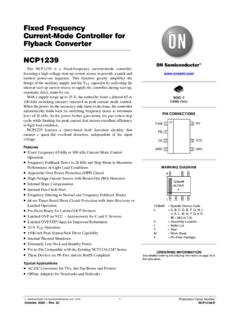
Transcription of UC3842B - High Performance Current Mode Controllers
1 Semiconductor Components Industries, LLC, 2013 September, 2013 Rev. 171 publication Order Number: UC3842B /DUC3842B, UC3843B,UC2842B, UC2843 BHigh PerformanceCurrent Mode ControllersThe UC3842B , UC3843B series are high Performance fixedfrequency Current mode Controllers . They are specifically designed forOff Line and DC DC converter applications offering the designer acost effective solution with minimal external components. Theseintegrated circuits feature a trimmed oscillator for precise duty cyclecontrol, a temperature compensated reference, high gain erroramplifier, Current sensing comparator, and a high Current totem poleoutput ideally suited for driving a power included are protective features consisting of input andreference undervoltage lockouts each with hysteresis, cycle by cyclecurrent limiting, programmable output deadtime, and a latch for singlepulse devices are available in an 8 pin dual in line and surfacemount (SOIC 8) plastic package as well as the 14 pin plastic surfacemount (SOIC 14).
2 The SOIC 14 package has separate power andground pins for the totem pole output UCX842B has UVLO thresholds of 16 V (on) and 10 V (off),ideally suited for off line converters. The UCX843B is tailored forlower voltage applications having UVLO thresholds of V (on) V (off).Features Trimmed Oscillator for Precise Frequency Control Oscillator Frequency Guaranteed at 250 kHz Current Mode Operation to 500 kHz Automatic Feed Forward Compensation Latching PWM for Cycle By Cycle Current Limiting Internally Trimmed Reference with Undervoltage Lockout High Current Totem Pole Output Undervoltage Lockout with Hysteresis Low Startup and Operating Current This is a Pb Free and Halide Free DeviceFigure 1. Simplified Block (12)VC7(11)Output6(10)PowerGround5(8)3(5 )CurrentSenseInputVref8(14)4(7)2(3)1(1)G ND5(9)RT/CTVoltageFeedbackInputRR+-VrefU ndervoltageLockoutOutputCompensationPin numbers in parenthesis are for the D suffix SOIC 14 14D SUFFIXCASE 751A1 See detailed ordering and shipping information in the packagedimensions section on page 17 of this data INFORMATIONSee general marking information in the device markingsection on page 19 of this data MARKING INFORMATION18 PDIP 8N SUFFIXCASE 626 PIN CONNECTIONSC ompensationNCVoltage FeedbackNCCurrent SenseNCRT/CTCompensationVoltage FeedbackCurrent SenseRT/CTVrefVrefNCVCCVCO utputGNDP ower GroundVCCO utputGND(Top View)876512341234141312115671098(Top View)SOIC 8D1 SUFFIXCASE 75118 , UC3843B, UC2842B, UC2843 RATINGSR atingSymbolValueUnitBias and Driver Voltages (Zero Series Impedance, see also Total Device spec)
3 VCC, VC30 VTotal Power Supply and Zener Current (ICC + IZ)30mAOutput Current , Source or Energy (Capacitive Load per Cycle) Sense, Voltage Feedback, Vref and Rt/Ct InputsVin to + to + to VCC orVC + Amp Output Sink CurrentIO10mAPower Dissipation and Thermal CharacteristicsD Suffix, Plastic Package, SOIC 14 Case 751 AMaximum Power Dissipation @ TA = 25 CThermal Resistance, Junction to AirD1 Suffix, Plastic Package, SOIC 8 Case 751 Maximum Power Dissipation @ TA = 25 CThermal Resistance, Junction to AirN Suffix, Plastic Package, Case 626 Maximum Power Dissipation @ TA = 25 CThermal Resistance, Junction to C/WmW C/WW C/WOperating Junction TemperatureTJ+150 COperating Ambient TemperatureUC3842B, UC3843 BUC2842B, UC2843 BUC2843 DUC3842BV, UC3843 BVTA0 to 70 25 to + 85 40 to +85 40 to +105 CStorage Temperature RangeTstg 65 to +150 CStresses exceeding Maximum Ratings may damage the device. Maximum Ratings are stress ratings only.
4 Functional operation above theRecommended Operating Conditions is not implied. Extended exposure to stresses above the Recommended Operating Conditions may affectdevice This device series contains ESD protection and exceeds the following tests:Human Body Model 4000 V per jedec Standard JESD22-A114 BMachine Model Method 200 V per jedec Standard JESD22-A115-A2. This device contains latch-up protection and exceeds 100 mA per jedec Standard JESD78UC3842B, UC3843B, UC2842B, UC2843 CHARACTERISTICS (VCC = 15 V [Note 3], RT = 10 k, CT = nF. For typical values TA = 25 C, for min/max valuesTA is the operating ambient temperature range that applies [Note 4], unless otherwise noted.)UC284XB, UC2843 DUC384XB, XBVC haracteristicsSymbolMinTypMaxMinTypMaxUn itREFERENCE SECTIONR eference Output Voltage (IO = mA, TJ = 25 C) Regulation (VCC = 12 V to 25 V)Regline Regulation (IO = mA to 20 mA)Regload StabilityTS mV/ CTotal Output Variation over Line, Load, and Noise Voltage (f = 10 Hz to 10 kHz, TJ = 25 C)Vn 50 50 mVLong Term Stability (TA = 125 C for 1000 Hours)S mVOutput Short Circuit CurrentISC 30 85 180 30 85 180mAOSCILLATOR SECTIONF requencyTJ = 25 CTA = Tlow to ThighTJ = 25 C (RT = k, CT = nF)fOSC494822552 2505556275494822552 2505556275kHzFrequency Change with Voltage (VCC = 12 V to 25 V)DfOSC/DV Change with Temperature, TA = Tlow to ThighDfOSC/DT %Oscillator Voltage Swing (Peak to Peak)VOSC VDischarge Current (VOSC = V)TJ = 25 C, TA = Tlow to ThighUC284XB, UC384 XBUC2843D, AMPLIFIER SECTIONV oltage Feedback Input (VO = V)
5 Bias Current (VFB = V)IIB Loop Voltage Gain (VO = V to V)AVOL6590 6590 dBUnity Gain Bandwidth (TJ = 25 C) MHzPower Supply Rejection Ratio (VCC = 12 V to 25 V)PSRR6070 6070 dBOutput CurrentSink (VO = V, VFB = V)Source (VO = V, VFB = V) mAOutput Voltage SwingHigh State (RL = 15 k to ground, VFB = V)Low State (RL = 15 k to Vref, VFB = V)UC284XB, UC384 XBUC2843D, Adjust VCC above the Startup threshold before setting to 15 Low duty cycle pulse techniques are used during test to maintain junction temperature as close to ambient as = 0 C for UC3842B , UC3843B; 25 C for UC2842B, UC2843B; 40 C for UC3842BV, UC3843BV, UC2843 DThigh = +70 C for UC3842B , UC3843B; +85 C for UC2842B, UC2843B, UC2843D; +105 C for UC3842BV, UC3843 BVUC3842B, UC3843B, UC2842B, UC2843 CHARACTERISTICS (VCC = 15 V [Note 7], RT = 10 k, CT = nF. For typical values TA = 25 C, for min/max valuesTA is the operating ambient temperature range that applies [Note 8], unless otherwise noted.)
6 UC284XB, UC2843 DUC384XB, XBVC haracteristicsSymbolMinTypMaxMinTypMaxUn itCURRENT SENSE SECTIONC urrent Sense Input Voltage Gain (Notes 5 and 6)UC2843D, UC284XB, Current Sense Input Threshold (Note 5)UC2843D, UC284XB, Supply Rejection Ratio (VCC = 12 V to 25 V, Note 5)PSRR 70 70 dBInput Bias CurrentIIB 10 10mAPropagation Delay ( Current Sense Input to Output)tPLH(In/Out) 150300 150300nsOUTPUT SECTIONO utput VoltageLow State (ISink = 20 mA)(ISink = 200 mA)UC284XB, UC384 XBUC384 XBV, UC2843 DHigh State(ISource = 20 mA)UC284XB, UC384 XBUC384 XBV, UC2843D(ISource = 200 mA)VOLVOH 13 VOutput Voltage with UVLO Activated (VCC = V, ISink = mA)VOL(UVLO) Voltage Rise Time (CL = nF, TJ = 25 C)tr 50150 50150nsOutput Voltage Fall Time (CL = nF, TJ = 25 C)tf 50150 50150nsUNDERVOLTAGE LOCKOUT SECTIONS tartup Threshold (VCC)UCX842B, BVUCX843B, BV, Operating Voltage After Turn On (VCC)UCX842B, BVUCX843B, BV, DVCC(min) SECTIONDuty CycleMaximum UC284XB, UC384XB, UC2843 DMaximumUC384 XBVM inimumDC(max)DC(min)94 96 09493 9696 0%TOTAL DEVICEP ower Supply CurrentStartup (VCC = V for UCX843B, UC2843 DStartupVCC 14 V for UCX842B, BV)(Note 7)ICC + IC Supply Zener Voltage (ICC = 25 mA)VZ3036 3036 V5.
7 This parameter is measured at the latch trip point with VFB = 0 Comparator gain is defined as: AVDV Output CompensationDV Current Sense Input7. Adjust VCC above the Startup threshold before setting to 15 Low duty cycle pulse techniques are used during test to maintain junction temperature as close to ambient as = 0 C for UC3842B , UC3843B; 25 C for UC2842B, UC2843B; 40 C for UC3842BV, UC3843BV, UC2843 DThigh = +70 C for UC3842B , UC3843B; +85 C for UC2842B, UC2843B, UC2843D; +105 C for UC3842BV, UC3843 BVUC3842B, UC3843B, UC2842B, UC2843 , TIMING RESISTOR (k ) M500 k200 k100 k50 k20 k10 kfOSC, OSCILLATOR FREQUENCY (kHz)VCC = 15 VTA = 25 CFigure 2. Timing Resistorversus Oscillator FrequencyFigure 3. Output Deadtimeversus Oscillator M500 k200 k100 k50 k20 k10 kfOSC, OSCILLATOR FREQUENCY (kHz) DT, PERCENT OUTPUT DEADTIME12 Figure 4. Oscillator Discharge Currentversus TemperatureFigure 5. Maximum Output Duty Cycleversus Timing Resistor, DISCHARGE Current (mA) 55TA, AMBIENT TEMPERATURE ( C)- = 15 VVOSC = V, MAXIMUM OUTPUT DUTY CYCLE (%) , TIMING RESISTOR (kW) = 15 VCT = nFTA = 25 C1.
8 CT = 10 nF2. CT = nF3. CT = nF4. CT = nF5. CT = 500 pF6. CT = 200 pF7. CT = 100 pF5 Idischg = mA7364 VCC = 15 VTA = 25 CFigure 6. Error Amp Small SignalTransient ResponseFigure 7. Error Amp Large SignalTransient ms/DIV20 mV/DIV20 VVCC = 15 VAV = = 25 CVCC = 15 VAV = = 25 CUC3842B, UC3843B, UC2842B, UC2843 8. Error Amp Open Loop Gain andPhase versus FrequencyFigure 9. Current Sense Input Thresholdversus Error Amp Output VoltageFigure 10. Reference Voltage Changeversus Source CurrentFigure 11. Reference Short Circuit Currentversus Temperature- 20 AVOL, OPEN LOOP VOLTAGE GAIN (dB)10 M10f, FREQUENCY (Hz)GainPhaseVCC = 15 VVO = V to VRL = 100 KTA = 25 k10 k100 M020406080100, EXCESS PHASE (DEGREES) 0VO, ERROR AMP OUTPUT VOLTAGE (V)0, Current SENSE INPUT THRESHOLD (V) = 15 VTA = 25 CTA = -55 CTA = 125 C VCC = 15 V TA = -55 C TA = 25 C, REFERENCE VOLTAGE CHANGE (mV)-160 Iref, REFERENCE SOURCE Current (mA)20406080100120refV-12- - 20- 24 TA = 125 C VCC = 15 VRL W, REFERENCE SHORT CIRCUIT Current (mA)SCI50- 55TA, AMBIENT TEMPERATURE ( C)- 2502550751001257090110 Figure 12.
9 Reference Load RegulationFigure 13. Reference Line ms/DIVVCC = 15 VIO = mA to 20 mATA = 25 CVCC = 12 V to 25 TA = 25 C, OUTPUT VOLTAGE CHANGE ( mV/DIV)VO , OUTPUT VOLTAGE CHANGE ( mV/DIV)VO UC3842B , UC3843B, UC2842B, UC2843 Sink Saturation(Load to VCC) TA = - 55 C VCC Source Saturation(Load to Ground)0 Vsat, OUTPUT SATURATION VOLTAGE (V)8000IO, OUTPUT LOAD Current (mA) TA = - 55 CFigure 14. Output Saturation Voltageversus Load CurrentFigure 15. Output WaveformFigure 16. Output Cross ConductionFigure 17. Supply Current versus Supply Voltage TA = 25 C RT = 10 kCT = nFVFB = 0 VISense = 0 VTA = 25 C, SUPPLY Current (mA)CCI00 VCC, SUPPLY VOLTAGE (V)10203040510152025 UCX843 BUCX842B TA = 25 C GND VCC = 15 V80 ms Pulsed Load120 Hz RateVCC = 30 VCL = 15 pFTA = 25 CVCC = 15 VCL = nFTA = 25 C50 ns/DIV100 ns/DIV100 mA/DIV20 V/DIV90%10%, OUTPUT VOLTAGEOV, SUPPLY CURRENTCCIPIN FUNCTION DESCRIPTION 8 Pin14 PinFunctionDescription11 CompensationThis pin is the Error Amplifier output and is made available for loop is the inverting input of the Error Amplifier.
10 It is normally connected to the switching powersupply output through a resistor voltage proportional to inductor Current is connected to this input. The PWM uses thisinformation to terminate the output switch Oscillator frequency and maximum Output duty cycle are programmed by connecting resistorRT to Vref and capacitor CT to ground. Operation to 500 kHz is pin is the combined control circuitry and power output directly drives the gate of a power MOSFET. Peak currents up to A are sourcedand sunk by this pin is the positive supply of the control is the reference output. It provides charging Current for capacitor CT through resistor pin is a separate power ground return that is connected back to the power source. It is usedto reduce the effects of switching transient noise on the control Output high state (VOH) is set by the voltage applied to this pin. With a separate powersource connection, it can reduce the effects of switching transient noise on the control pin is the control circuitry ground return and is connected back to the power source ,4,6,13 NCNo connection.
