Transcription of XR-2206 - SparkFun Electronics
1 Analog plus companyTMMonolithicFunction GeneratorRev. 2008 EXAR Corporation, 48720 Kato Road, Fremont, CA 94538 (510) 668-7000 (510) 668-70171 February 2008-8 FEATURES Low-Sine Wave Distortion, , Typical Excellent Temperature Stability, 20ppm/ C, Typ. Wide Sweep Range, 2000:1, Typical Low-Supply Sensitivity, , Typ. Linear Amplitude Modulation TTL Compatible FSK Controls Wide Supply Range, 10V to 26V Adjustable Duty Cycle, 1% TO 99%APPLICATIONS Waveform Generation Sweep Generation AM/FM Generation V/F Conversion FSK Generation Phase-Locked Loops (VCO)GENERAL DESCRIPTIONThe XR-2206 is a monolithic function generatorintegrated circuit capable of producing high quality sine,square, triangle, ramp, and pulse waveforms ofhigh-stability and accuracy.
2 The output waveforms can beboth amplitude and frequency modulated by an externalvoltage. Frequency of operation can be selectedexternally over a range of to more than circuit is ideally suited for communications,instrumentation, and function generator applicationsrequiring sinusoidal tone, AM, FM, or FSK generation. Ithas a typical drift specification of 20ppm/ C. The oscillatorfrequency can be linearly swept over a 2000:1 frequencyrange with an external control voltage, while maintaininglow INFORMATIONPart RangeXR-2206P16 Lead 300 Mil PDIP 40 C to +85 CXR-2206CP16 Lead 300 Mil PDIP0 C to +70 CXR-2206D16 Lead 300 Mil JEDEC SOIC0 C to +70 CXR-22062 Rev.
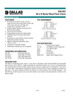
3 SYNCOVCO4 VCC12 GND10 BIAST imingCapacitor5TC16TC2 TimingResistors7TR18TR29 FSKI1 AMSIC urrentSwitchesMultiplierAnd SineShaper2 STO3MO13 WAVEA114 WAVEA215 SYMA116 SYMA2 Figure 1. XR-2206 Block Diagram+1XR-22063 Rev. Lead PDIP, CDIP ( )SYMA2 SYMA1 WAVEA2 WAVEA1 GNDSYNCOBIASFSKIAMSISTOMOVCCTC1TC2TR1TR2 12345678161514131211109 AMSISTOMOVCCTC1TC2TR1TR2 SYMA2 SYMA1 WAVEA2 WAVEA1 GNDSYNCOBIASFSKI16 Lead SOIC (Jedec, )16198234567151413121110 PIN DESCRIPTIONPin #SymbolTypeDescription1 AMSIIA mplitude Modulating Signal or Triangle Wave Power Capacitor Capacitor Resistor 1 Resistor 2 Shift Keying Voltage Output.
4 This output is a open collector and needs a pull up resistor to Form Adjust Input Form Adjust Input Symetry Adjust Symetry Adjust ELECTRICAL CHARACTERISTICSTest Conditions: Test Circuit of Figure 2 Vcc = 12V, TA = 25 C, C = F, R1 = 100k , R2 = 10k , R3 = 25k Unless Otherwise Specified. S1 open for triangle, closed for sine CharacteristicsSingle Supply Voltage10261026 VSplit-Supply Voltage+5+13+5+13 VSupply Current121714 20mA R1 10k Oscillator SectionMax. Operating = 1000pF, R1 = 1k Lowest Practical = 50 F, R1 = 2M Frequency Accuracy+1+4+2% of fofo = 1/R1 CTemperature StabilityFrequency+10+50+20ppm/ C0 C TA 70 CR1 = R2 = 20k Sine Wave Amplitude Stability248004800ppm/ CSupply = 10V, VHIGH = 20V,R1 = R2 = 20k Sweep Range1000:12000:12000:1fH = fLfH @ R1 = 1k fL @ R1 = 2M Sweep Linearity 10:1 Sweep22%fL = 1kHz, fH = 10kHz 1000:1 Sweep88%fL = 100Hz, fH = 100kHz FM +10% DeviationRecommended Timing Components Timing Capacitor: FFigure 5 Timing Resistors.
5 R1 & R21200012000k Triangle Sine Wave Output1 Figure 3 Triangle Amplitude160160mV/k Figure 2, S1 Open Sine Wave Amplitude40608060mV/k Figure 2, S1 Closed Max. Output Swing66Vp-p Output Impedance600600 Triangle Linearity11% Amplitude 1000:1 SweepSine Wave Distortion Without = 30k With Figure 7 and Figure 8 Notes1 Output amplitude is directly proportional to the resistance, R3, on Pin 3. See Figure maximum amplitude stability, R3 should be a positive temperature coefficient face parameters are covered by production test and guaranteed over operating temperature ELECTRICAL CHARACTERISTICS (CONT D) XR-2206 PXR-2206 ModulationInput Impedance5010050100k Modulation Range100100%Carrier Suppression5555dBLinearity22%For 95% modulationSquare-Wave OutputAmplitude1212Vp-pMeasured at Pin Time250250nsCL = 10pFFall Time5050nsCL = 10pFSaturation = 2mALeakage AVCC = 26 VFSK Keying Level (Pin 9)
6 Section on circuit controlsReference Bypass at Pin amplitude is directly proportional to the resistance, R3, on Pin 3. See Figure maximum amplitude stability, R3 should be a positive temperature coefficient face parameters are covered by production test and guaranteed over operating temperature are subject to change without noticeABSOLUTE MAXIMUM RATINGSP ower Supply26V.. Power Dissipation750mW.. Derate Above 25 C5mW/ C.. Total Timing Current6mA.. Storage Temperature-65 C to +150 C.. SYSTEM DESCRIPTIONThe XR-2206 is comprised of four functional blocks; avoltage-controlled oscillator (VCO), an analog multiplierand sine-shaper; a unity gain buffer amplifier; and a set ofcurrent VCO produces an output frequency proportional toan input current, which is set by a resistor from the timingterminals to ground.
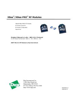
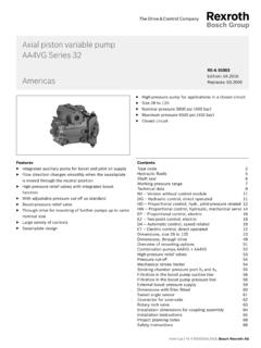
7 With two timing pins, two discreteoutput frequencies can be independently produced forFSK generation applications by using the FSK inputcontrol pin. This input controls the current switches whichselect one of the timing resistor currents, and routes it tothe 5 Figure 2. Basic Test CircuitSymmetry Adjust25K 1 6 7 8 9113213141516410 12XR-22061mFVCCCR1R2 FSK InputS1 THD Adjust500 Triangle OrSine WaveOutputSquare +1 VCO+S1 = Open For Triangle= Closed For SinewaveFigure 3. Output Amplitudeas a Function of the Resistor,R3, at Pin 3 TriangleSinewave2622181410812 16 20 24 2870 C 4.
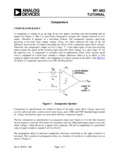
8 Supply Current vsSupply Voltage, Timing, R020406080100123456 Peak Output Voltage (Volts)R3 in (KW)I CC(mA)VCC (V)XR-22067 Rev. MINIMUM TIMING R Figure 5. R versus Oscillation Frequency. 4V4V10M1M100K10K1K10-210102 MAXIMUM TIMING RVCC / 2DC Voltage At Pin 1 Frequency (Hz)Timing Output AmplitudeFigure 6. Normalized Output Amplitude versus DC Bias at AM Input (Pin 1)Figure 7.
9 Trimmed Distortion versusTiming (%)Timing R K(W) C = For MinimumDistortion At 30 KWFigure 8. Sine Wave Distortion versus Operating Frequency with Timing Capacitors (%)Frequency (Hz) R=3KW RL=10KW NORMAL RANGE TYPICAL VALUE= Pin 2 VOUT()104106XR-22068 Rev. 9. Frequency Drift FR=1M R=2K R=10K R=200K R=1M R=1K R=10K R=2K R=1K Ambient Temperature (C )Figure 10. Circuit Connection for Frequency +-VCRIBICRcITPin 7or 812 100 Figure 11. Circuit tor Sine Wave Generation without External Adjustment.(See Figure 3 for Choice of R3)R=200K Frequency Drift (%)+- 1 5 6 7 8 9113213141516410 1 2XR-22061 FCR12M1KS1 Triangle OrSine Wave OutputSquare F1 +1++VCOS1 Closed For Sinewave3 VXR-22069 Rev.
10 12. Circuit for Sine Wave Generation with Minimum Harmonic Distortion. (R3 Determines Output Swing - See Figure 3)Figure 13. Sinusoidal FSK GeneratorSymmetry Adjust25 KRB 1 5 6 7 8 91132131415164112XR-22061mFC1KR12MF =S1 Triangle OrSine Wave OutputSquare +++1 VCC 1 5 6 7 8 9113213141516410 12XR-22061mFVCCCFSK InputR1R2<1V>2VF1F2F1=1 +++1 CurrentSwitchesS1 Closed For Sinewave1 RCFSK OutputXR-220610 Rev. 14. Circuit for Pulse and Ramp Generation. 1 5 6 7 8 9113213141516410 +1++CurrentSwitchesf 2C 1R1 R2 R1R1 R2 Duty Cycle =Sawtooth OutputPulse OutputFrequency-Shift KeyingThe XR-2206 can be operated with two separate timingresistors, R1 and R2, connected to the timing Pin 7 and 8,respectively, as shown in Figure 13.