Transcription of Zen Variations #9 - FIRST WATT
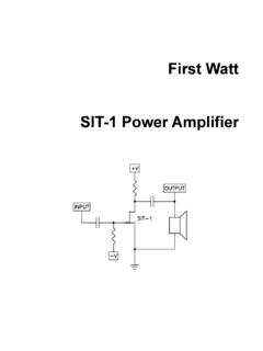
1 Zen Variations #9By Nelson PassIntroductionIn ZV8 we dipped our toes into the waters of power JFET transistors using thenew Lovoltech LU1014D in a simple circuit. The focus of the project was on theJFET itself, and except for a cascode transistor the rest of the amplifier usedonly passive components. Here in four installments we will increase thecomplexity of the circuitry around the JFET with an eye toward distortionperformance surpassing any of the Zen projects to date. Much of this project will make reference to ZV8 (AudioXpress, January 2006and ), which discusses the characteristics of the LU1014 Dpower JFET and the circuit that forms the basis for this project.
2 ZV8 alsobrought up the subject of load-line optimization, which we will exploit here,working the Drain to Source voltage (Vds) curve to reduce your quick reference, the most basic circuit is presented here as Figure 1 Supply Filter and Constant Current SourceWe bias ZV8 with a pair of light bulbs, whose resistance offers about 11 ohmsand delivers about amps to the gain transistor. This has three drawbacks:1) It is inefficient - the power supply must have about 50% higher voltagethan the amplifier s peak ) The light bulb resistances parallel the load, so that an 8 ohm load lookslike ohms, making the gain device work nearly twice as hard andraising the ) It has poor power supply noise rejection a portion of the noise in thepower supply comes through the light bulbs to the , we will put in an active supply filter to reduce power supply noise and turn-on thump.
3 Then we will replace the light bulbs with a 2 amp constant currentsource. It will not glow warmly on cold winter evenings, but it will draw lesscurrent, deliver about 50% more power, and has lower distortion and 2 shows the replacement of the two light bulbs with the supply filter andthe constant current source. Q4 is set up as a capacitance multiplier whose C3and R8 time constant is set to 5 seconds. At this charge rate, the circuit will seeminimal supply ripple and have a low turn-on transient. The supply voltageappearing on the Drain of Q3 enjoys some additional passive filtering from C2and C6.
4 Q4 drops about 4 volts off the supply, so that a 50V unregulated raildelivers about 46 volts at the Drain of Q3 (Voltages in all schematics areapproximate). We could DC stabilize the supply with zener diodes across C3,but that would make it more difficult to have such a slow turn-on, so we will usethe constant current source to DC stabilize the bias constant current source is formed by N channel Mosfet Q3 controlled byNPN transistor Q5. We make use of the physical constant of the PN junction ofthe Base-Emitter voltage of Q5 for a reference, and the circuit works to maintainabout .66 volts across the resistors R4 through R6, which makes for a constantcurrent of 2 amps.
5 R10 through R13 are there to provide a relatively constantbias current for the Collector of Q5, with C4 bootstrapping from the are few other changes to the circuit of Figure 1, but you will note theaddition of an audiophile-approved bypass capacitor on the output, andvariability in the value of R3. Later we will see that that this value can be usedto optimize the performance around the characteristics of individual Figure 2 we trim the value of P1 for a Drain voltage of one-half the supplyvoltage by adjusting the Vds of the JFET if the voltage on the Drain of Q3 is46 volts, then we want about 23 volts on the Drain of Q2.
6 With the appropriatevalue for R3 (approximately 2 ohms) we will see minimum distortion and a Vdsacross the JFET Q1 of 2 to 3 volts. This comes out to about 4 to 6 wattsdissipation for the particular circuit is a transconductance amplifier, that is to say a currentsource whose output impedance is mostly determined by the 100 ohm outputresistor R7. To lower the output impedance we will later apply some 3 shows the comparative performance of the circuits of Figure 1 and 2,and we see an immediate distortion reduction by about half. What is less clearis that the light bulb version is clipping at about 10% distortion at 10 watts, whilethe current source circuit clips comparably at about 20 2 Cascode ModulationIn ZV8 we spent some time discussing the triode-like character of the powerJFET at low voltages, where both the transconductance and plate (Vds)characteristics show exponential behaviour.
7 With such a device, you canexploit distortion cancellation by carefully choosing the load line of operation sothat the variation in gain versus current is cancelled against the gain versusvoltage so that the distortion of the device is dramatically phenomenon was only discussed in ZV8, and here is where we will put it touse. In many examples, correctly varying the Vds versus Ids (Drain-Sourcecurrent) in the JFET would involve more complex circuitry, but on this rareoccasion Mother Nature does us a favor. The optimal voltage variation can behad across resistors R1 R3 which are coincidentally close to the valueselected to give the JFET the correct DC self-biased value at 2 Figure 2 C5 is placed so that the AC voltage at the Source of Q2 tracks theSource of Q1, holding the Vds of Q1 at a relatively constant DC value of about 2to 3 volts.
8 This is classic cascode operation. But a truly constant Vds for Q1 isnot the lowest distortion load line for the device. Because we want to canceltwo nonlinear characteristics, the optimal Vds across Q1 will be DC plus a finiteAC voltage at around -600 mV per amp, which was determined by testing at 1watt. In figure 4 we achieve this by grounding one leg of C5 - the simplestchange imaginable. Figure 5 shows the 3 Negative FeedbackThe FIRST two alterations improve the 1- watt performance by an order ofmagnitude, but it s still a current source. You might elect to stop here if acurrent source meets your needs.
9 If you want a damping factor, we will applysome loop feedback, as seen in Figure 6 is different from Figure 4 with R16, R17 and C8 forming a negativefeedback loop. Like most of its Zen predecessors, ZV9 uses feedback to lowerthe output impedance. Roughly, R17 divided by R16 determines the gain andR16 determines the input impedance. With the values shown we use about 10dB of feedback to get a damping factor of about 3 and a distortion reduction ofabout half. C8 imposes a small amount of compensation that makes the squarewave look good. Figure 7 shows the comparison with and without that the improvement is not uniform with simple low feedback circuits itoften is 4 The Aleph Current SourceThose familiar with ZV4 will probably figure out why I chose the particularcurrent source of Figure 2 - it easily converts to the non-constant current sourceused in the Aleph series of amplifiers and as described in patent # 5,710, describes this current source in greater detail, but referring to Figure 8, thecurrent source has the addition of C9, R18 and R19 that set the current sourceAC value to track an arbitrary fraction of the output.
10 Usually we set this valuearound 50%, and we can use it to ghost the complex load impedance at anegative multiple of the load value. With the values chosen in Figure 8, an 8ohm load would look like 16 ohms to the JFET gain device. By raising theapparent load impedance, the current source lowers the distortion of Q1 whilestill leaving it in control of the output. With tubes, Variations of this idea havebeen called SRPP and SEPP output stages, although the distinction betweenan input and output stage is somewhat blurred in a single stage one watt , the improvement is a factor of about 5, and at 10 watts a factor ofabout 10.