Transcription of Zynq UltraScale+ RFSoC RF Data Converter v2.4 Gen 1/2/3 ...
1 Zynq UltraScale+ RFSoC RFData Converter Gen1/2/3 LogiCORE IP Product GuideVivado Design SuitePG269 ( ) November 30, 2020 Table of ContentsChapter 1: IP 2: Content by Design and 3: Product 4: Designing with the Core Configuration in the Vivado Design Modulator Correction ..139 Coarse Update Mode (Gen 3)..165PG269 ( ) November 30, 2020 UltraScale+ RFSoC RF data Converter Gen 1/2/3 2 Send FeedbackBitstream to the AXI4-Stream 5: Design Flow and Generating the and 212 Chapter 6: Example 213RF-ADC data Capture 214RF-DAC data Stimulus data 7: Test 222 Appendix A: 225 Changes from to from to from to from to from to from to B: Help on 230 Debug 232 Appendix C: Zynq UltraScale+ RFSoC RF data Converter Bare-metal/Linux API ( ) November 30, 2020 UltraScale+ RFSoC RF data Converter Gen 1/2/3 3 Send FeedbackAppendix D: RF E: Additional Resources and Legal Navigator and Design Read.
2 Important Legal 345PG269 ( ) November 30, 2020 UltraScale+ RFSoC RF data Converter Gen 1/2/3 4 Send FeedbackChapter 1IP FactsThe Xilinx LogiCORE IP Zynq UltraScale+ RFSoC RF data Converter IP core provides aconfigurable wrapper to allow the RF-DAC and RF-ADC blocks to be used in IP ! In this guide reference is made to the Dual and Quad RF-ADC and RF-DAC tiles; for theactual sampling rate specifications, see the Zynq UltraScale+ RFSoC data Sheet: DC and AC SwitchingCharacteristics (DS926 ). Note that Dual and Quad refers to the tile configuration and not the number Up to 16 14-bit RF-DACs Gen 1/Gen 2: Four 12-bit Dual RF-ADC tiles, or four 12-bit Quad RF-ADC tiles Gen 3: Two or four 14-bit Dual RF-ADC tiles, and/or two or four 14-bit Quad RF-ADC tiles Supports alignment between multiple converters (Multi-Tile Synchronization (MTS)) Pre-programs RF-DAC and RF-ADC with key user-defined parameters Multiple AXI4-Stream data interfaces for RF-ADCs and RF-DACs Single AXI4-Lite configuration interface Gen 1/Gen 2: 1x (bypass), 2x, 4x, 8x decimation and interpolation Gen 3.
3 1x (bypass), 2x, 3x, 4x, 5x, 6x, 8x, 10x, 12x, 16x, 20x, 24x, 40x decimation andinterpolation with additional 2x interpolation after mixer digital complex mixers and Numerical Controlled Oscillator (NCO) Quadrature Modulation Correction (QMC) Gen 3: Embedded digital Step Attenuator (DSA) for each RF-ADC, and Variable Output Power(VOP) control for each RF-DAC On-chip PLL and VCO per tile Gen 3: On-chip clock distribution network Gen 3: TDD mode support power saving mode and RX/Obs sharing modeChapter 1: IP FactsPG269 ( ) November 30, 2020 UltraScale+ RFSoC RF data Converter Gen 1/2/3 5 Send FeedbackIP FactsLogiCORE IP Facts TableCore SpecificsSupported Device Family1 Zynq UltraScale+ RFSoCSupported User InterfacesAXI4-Stream, AXI4-Lite Control/StatusResourcesPerformance and Resource Use web pageProvided with CoreDesign FilesRTLE xample DesignVerilogTest BenchVerilogConstraints FileXilinx Design Constraints (XDC)Simulation ModelVerilogSupported S/W Driver2 Standalone and LinuxTested Design Flows3 Design EntryVivado IP IntegratorSimulationFor supported simulators, see the Xilinx Design Tools: Release Notes SynthesisSupportRelease Notes and Known IssuesMaster Answer Record: 69907 All Vivado IP Change LogsMaster Vivado IP Change Logs: 72775 Xilinx Support web pageNotes:1.
4 For a complete list of supported devices, see the Vivado IP Stand-alone driver details can be found in the software development kit <Install Directory>/Vitis/<Release>/ data /embeddedsw/ documentation is available in Appendix C: Zynq UltraScale+ RFSoC RF data Converter Bare-metal/Linux For the supported versions of third-party tools, see the Xilinx Design Tools: Release Notes 1: IP FactsPG269 ( ) November 30, 2020 UltraScale+ RFSoC RF data Converter Gen 1/2/3 6 Send FeedbackChapter 2 OverviewThe Xilinx Zynq UltraScale+ RFSoC family integrates the key subsystems required toimplement a complete software-defined radio including direct RF sampling data converters,enabling eCPRI and Gigabit Ethernet-to-RF on a single, highly programmable RFSoC offers multiple RF-sampling analog -to- digital (RF-ADC) and RF-sampling digital -to- analog (RF-DAC) data converters.
5 The data converters are high-precision, high-speed and power-efficient. Both are highly configurable and tightly integrated with the programmable logic (PL)resources of the Zynq UltraScale+ RF-ADC supports device-dependent sample rates and input signal frequencies listed in theZynq UltraScale+ RFSoC data Sheet: Overview (DS889), with excellent dynamic range RF-DAC generates output carrier frequencies at rates defined in the Zynq UltraScale+ RFSoCData Sheet: DC and AC Switching Characteristics (DS926), depending on the device (see the ZynqUltraScale+ RFSoC data Sheet: Overview (DS889) for device RF data converters also include power efficient digital down converters (DDCs) and digital upconverters (DUCs) that include programmable interpolation and decimation rates, a numericallycontrolled oscillator (NCO), and a complex mixer.)
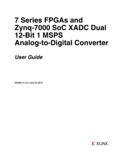
6 The DDCs and DUCs can also support multi-band operation. The following figure shows the block diagram of the Zynq UltraScale+ RFSoCRF data RF-ADCs and RF-DACs are organized into tiles, each containing one, two, or four RF-ADCsor one, two, or four RF-DACs. Multiple tiles are available in each Zynq UltraScale+ RFSoC (seethe specific device data sheet for the number of tiles and converters per device). Each tile alsoincludes a block with a PLL and all the necessary clock handling logic and distribution routing forthe analog and digital guide describes the Zynq UltraScale+ RFSoC RF data Converter IP core and softwaredrivers that are used to configure the data converters and instantiate them for use in a this guide, reference is made to the Dual and Quad RF-ADCs, and the Dual (Gen 3) and QuadRF-DACs; for the actual sampling rate specifications see the Zynq UltraScale+ RFSoC data Sheet:DC and AC Switching Characteristics (DS926).
7 For device specifications and additional information, see: Zynq UltraScale+ RFSoC data Sheet: Overview (DS889) Zynq UltraScale+ RFSoC data Sheet: DC and AC Switching Characteristics (DS926)Chapter 2: OverviewPG269 ( ) November 30, 2020 UltraScale+ RFSoC RF data Converter Gen 1/2/3 7 Send Feedback Zynq UltraScale+ Device Technical Reference Manual (UG1085).Figure 1: Zynq UltraScale+ RFSoC RF data Converter IP Core in Zynq UltraScale+ RFSoC (Gen 1/Gen 2/Gen 3)Zynq UltraScale+ RFSoCControl and ConfigurationData Converter IP CoreProcessing SystemQuad ARM Cortex-A53 Dual ARM Cortex-R5 GTY SerialTransceiversProgrammableLogicDUCAX I4-StreamDUCAXI4-Stream4 to 16 TX ChannelsDDCAXI4-StreamDDCAXI4-Stream4 to 16 RX ChannelsAXI4-LiteDACDACADCADCX19532-0628 19 Navigating Content by Design ProcessXilinx documentation is organized around a set of standard design processes to help you findrelevant content for your current development task.
8 This document covers the following designprocesses: Hardware, IP, and Platform Development: Creating the PL IP blocks for the hardwareplatform, creating PL kernels, subsystem functional simulation, and evaluating the Vivado timing, resource use, and power closure. Also involves developing the hardware platform forsystem integration. Topics in this document that apply to this design process include: Port Descriptions Register SpaceChapter 2: OverviewPG269 ( ) November 30, 2020 UltraScale+ RFSoC RF data Converter Gen 1/2/3 8 Send Feedback Customizing and Generating the Core Appendix C: Zynq UltraScale+ RFSoC RF data Converter Bare-metal/Linux DriverConventionsThis document covers different aspects of the Zynq UltraScale+ RF data Converter hardware,IP, software driver, and covers Gen 3 devices. The following naming conventions are used forconvenience, conciseness, and clear information document uses Gen x to distinguish different generations of the Zynq UltraScale+ RFData Converter family as below: Gen 1: XCZU2xDR Gen 2: XCZU39DR Gen 3: XCZU4xDRIn this document, items that are specific to Gen 3 are clearly identified as Gen and Quad RF-ADC/RF-DAC TilesThere are two types of Converter tiles for the RF-ADCs, called Dual and Quad tiles.
9 For RF-ADCs,the converters in the Dual tiles have different maximum sampling rates and different interleavingfactors to the Quad tiles. Gen 1 and Gen 3 devices have both type of tiles, while Gen 2 devicesconsist of Quad RF-ADC tiles RF-DAC tiles are available in Gen 1/Gen 2 devices and Dual RF-DAC tiles are additionallyavailable in Gen 3 devices; the Dual RF-DAC tiles have two dedicated DUCs for each channel tosupport dual-band applications. There is no performance difference between converters in bothtypes of RF-DAC : In this document, colored table rows call attention to specific Gen 3 device 1: Tile ConfigurationTile TypeNumber ofConvertersDevice TypeNotesQuad RF-ADC4 Gen 1/Gen 2/Gen 3 Each RF-ADC has an interleaving factor of RF-ADC2 Gen 1/Gen 3 Each RF-ADC has an interleaving factor of eight, hence doublethe sampling rate of the converters in the Quad RF-ADC RF-DAC4 Gen 1/Gen 2/Gen 3 Each RF-DAC has one dedicated 2: OverviewPG269 ( ) November 30, 2020 UltraScale+ RFSoC RF data Converter Gen 1/2/3 9 Send FeedbackTable 1: Tile Configuration (cont'd)Tile TypeNumber ofConvertersDevice TypeNotesDual RF-DAC2 Gen 3 Each RF-DAC has two dedicated DUCs.
10 For Gen 3 devicesfeaturing Quad RF-DACs or a combination of Quad and DualRF-DACs, all tiles have external clock : For Gen 3 devices with only Dual RF-DACs, the even tileshave external clock :1. Gen 3 devices with one RF-ADC per tile are considered as Dual RF-ADCs with the upper ADC (input VinX_23)unavailable. All data paths are available for use on these devices. These devices do not support I/Q input Gen 3 devices with one RF-DAC per tile are considered as Dual RF-DACs with the upper DAC (output VoutX2)unavailable. All data paths are available for use on these devices. These devices do not support I/Q output the Zynq UltraScale+ RFSoC data Sheet: Overview (DS889) for an overview of the maximumsampling rates and the Zynq UltraScale+ RFSoC data Sheet: DC and AC Switching Characteristics(DS926) for the exact following figures illustrate the tile 2: RF-ADC Tile StructureVinX0 ADCData PathmX0_axisVinX1 ADCData PathmX1_axisVinX2 ADCData PathmX2_axisVinX3 ADCData PathmX3_axisQuad RF-ADC TileADCData PathmX0_axisADCData PathmX2_axisDual RF-ADC Tile (Gen 1/3)VinX_01 VinX_23mX3_axismX1_axisQQX23275-102920 Chapter 2: OverviewPG269 ( ) November 30, 2020 UltraScale+ RFSoC RF data Converter Gen 1/2/3 10 Send FeedbackFigure 3.