Cmos Operational Amplifier Design
Found 7 free book(s)
TUTORIAL CADENCE DESIGN ENVIRONMENT - Anasayfa
web.itu.edu.trNow we are going to illustrate how to carry out the complete design flow shown in Fig. 1 using the Cadence tools. A simple Operational Transconductance Amplifier (OTA) will be designed in the AMI 0.5µm CMOS technology. However, the same procedures apply to complete chip designs. 5.1. Library creation and selection of technology
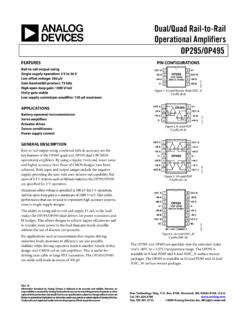
Dual/Quad Rail-to-Rail Operational Amplifiers OP295/OP495
www.analog.comoperational amplifiers. By using a bipolar front end, lower noise and higher accuracy than those of CMOS designs have been achieved. Both input and output ranges include the negative supply, providing the user with zero-in/zero-out capability. For users of 3.3 V systems such as lithium batteries, the OP295/OP495 are specified for 3 V operation.
ENGINEERING MATHEMATICS-III
vtu.ac.inand MOSFETs, Biasing MOSFETs, FET Applications, CMOS Devices. Wave-Shaping Circuits: Integrated Circuit(IC) Multivibrators. Introduction to Operational Amplifier : Ideal v/s practical Opamp, Performance Parameters, Operational Amplifier Application Circuits :Peak Detector
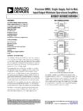
Precision CMOS, Single-Supply, Rail-to-Rail, Input/Output ...
www.analog.comPrecision CMOS, Single-Supply, Rail-to-Rail, Input/Output Wideband Operational Amplifiers Data Sheet AD8601/AD8602/AD8604 . Rev. I Document Feedback . Information furnished by Analog Devices is believed to be accurate and reliable. However, no responsibility is assume dby Analog Devices for its use, nor for any infringements of patents or other
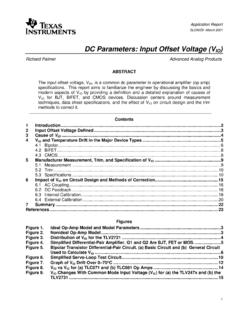
DC Parameters: Input Offset Voltage (V - Texas Instruments
www.ti.comThe input offset voltage, VIO, is a common dc parameter in operational amplifier (op amp) specifications. This report aims to familiarize the engineer by discussing the basics and modern aspects of VIO by providing a definition and a detailed explanation of causes of VIO for BJT, BiFET, and CMOS devices. Discussion centers around measurement
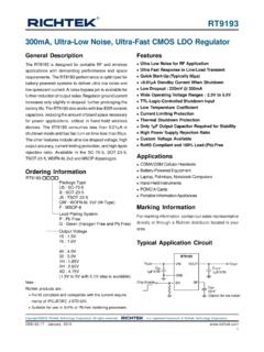
300mA, Ultra-Low Noise, Ultra-Fast CMOS LDO Regulator
www.richtek.com300mA, Ultra-Low Noise, Ultra-Fast CMOS LDO Regulator Marking Information For marking information, contact our sales representative directly or through a Richtek distributor located in your area. Ordering Information General Description The RT9193 is designed for portable RF and wireless applications with demanding performance and space ...
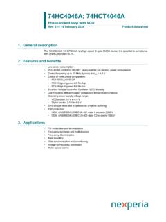
Phase-locked loop with VCO - Nexperia
assets.nexperia.comThe input signal can be coupled to the self-biasing amplifier at pin SIG_IN, when the signal swing is between the standard HC/T family input logic levels. Capacitive coupling is required for signals with smaller swings. 8.2.1. Phase Comparator 1 (PC1) This circuit is an EXCLUSIVE-OR network. The signal and comparator input frequencies (fi) must