Jfet Junction Field Effect Transistor
Found 10 free book(s)
International Transistor Equivalents Guide
worldradiohistory.comC complementary transistor NPN/PNP DG dual germanium transistor DJ dual junction transistor DS dual silicon transistor FET field effect transistor G germanium transistor GD germanium Darlington transistor J junction FET (JFET) M MOSFET ME multiple -emitter transistor MOS metal oxide semiconductor P photo -transistor PU programmable unijunction ...

Chapter 4 Junction Field Effect Transistor Theory and ...
staff.utar.edu.myJunction Field Effect Transistor Theory and Applications _____ 4.0 Introduction Like bipolar junction transistor, junction field effect transistor JFET is also a three-terminal device but it is a unipolar device, which shall mean that the current is made of either electron or hole carrier.
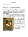
Variable Frequency Oscillators (VFOs)
www.qrparci.orgSecret # 1. Junction Field Effect Transistors (JFETs) The first secret of a stable VFO is using a JFET instead of a bipolar transistor. As described earlier, a field effect transistor is better because it is less sensitive to temperature. I have used 2N3823, 2N5484 and 2N4416 N-channel JFET’s for VFO oscillators.
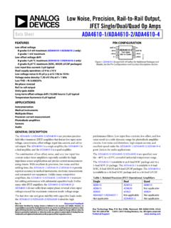
Low Noise, Precision, Rail-to-Rail Output, JFET Single ...
www.analog.comADA4610-1/ADA4610-2/ADA4610-4 are precision junction field effect transistor (JFET) amplifiers that feature low input noise voltage, current noise, offset voltage, input bias current, and rail -to-rail output. The ADA4610-1 is a single amplifier , the ADA4610-2 is a dual amplifier, and the ADA4610-4 is a quad amplifier.
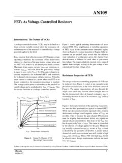
Introduction: The Nature of VCRs
www.vishay.comFor a junction field-effect transistor (JFET) under certain operating conditions, the resistance of the drain-source channel is a function of the gate-source voltage alone and the JFET will behave as an almost pure ohmic resistor. Maximum drain-source current, I DSS, and minimum re-sistance rDS(on), will exist when the gate-source voltage

Power MOSFET Basics
www.aosmd.comPower MOSFETs (Metal Oxide Semiconductor Field Effect Transistor) are the most commonly used power devices due to their low gate drive power, fast switching speed and superior paralleling capability. Most power MOSFETs feature a vertical structure with Source and Drain on opposite sides of the wafer in order to support higher current and voltage.

Spectre Circuit Simulator Reference
eece.cu.edu.egSpectre Circuit Simulator Reference September 2003 3 Product Version 5.0 MISN Field Effect Transistor (misnan ...
SMD-codes databook 2019 edition - Turuta
turuta.mdFor example, with a 6H SMD-code in a SOT-23 case might be either a npn-transistor BC818 (CDIL) or a capacitance-diode FMMV2104 (Zetex) or a n-channel jFET transistor MMBF5486 (Motorola) or a pnp-digital transistor MUN2131 (Motorola) or a pnp-digital transistor UN2117 (Panasonic) or a CMOS-integrated circuit- voltage detector with reset

Syllabus of M. Sc. in Physics
buruniv.ac.inshift, effect of magnetic field on the above spectra, Zeeman and Paschen-Back effect. (7 lectrures) 2. Spectra of divalent atoms: Singlet and triplet states of …

ディスクリート半導体の基礎
toshiba.semicon-storage.com(jfet) 抵抗内蔵型トランジスタ. 絶縁ゲートバイポーラトランジスタ. トランジスタ. トランジスタは、大別するとバイポーラ型、電界効果型および絶縁ゲートバイポーラ型の3種類に分 類される半導体デバイスです。