
AN5306 Introduction Application note - STMicroelectronics
defined using a set of analog multiplexers which interconnect the OPAMP input and output terminals through an internal resistor network. Final gain of this programmable gain amplifier (PGA) is defined by the resistor ratios on the feedback. Figure 3. Internal OPAMP connections in STM32G4 Series illustrates the basic schematic of the OPAMP
Download AN5306 Introduction Application note - STMicroelectronics

Information
Domain:
Source:
Link to this page:
Documents from same domain

Low-power dual operational amplifier - st.com
www.st.comFebruary 2016 DocID2471 Rev 17 1/24 This is information on a product in full production. www.st.com LM2904, LM2904A Low-power dual operational amplifier

AN3128 Application note - st.com
www.st.comJune 2011 Doc ID 16918 Rev 5 1/105 AN3128 Application note STM32 embedded graphic objects/touchscreen library Introduction This library is a firmware package which contains a collection of routines, data structures,

AN4767 Application note - st.com
www.st.comDocID028380 Rev 2 7/16 AN4767 Dual bank use cases 15 With dual bank, all the manipulation with the other bank is just another task of the main program.

AN3155 Application note - st.com
www.st.comOctober 2016 DocID17066 Rev 7 1/37 1 AN3155 Application note USART protocol used in the STM32 bootloader Introduction This application note describes the USART protocol used in the STM32 microcontroller

USB Power Delivery and Type-C - st.com
www.st.comUSB Type -C Overview USB Power Delivery specification introduces USB Type-C receptacle, plug and cable; they provide a smaller, thinner and more robust alternative to existing USB interconnect.

Datasheet - L78 - Positive voltage regulator ICs - …
www.st.comTO- 2 2 0 TO-2 2 0 F P DPAK D² PAK Features • Output current up to 1.5 A • Output voltages of 5; 6; 8; 8.5; 9; 12; 15; 18; 24 V • Thermal overload protection

AN2867 Application note - st.com
www.st.comMay 2017 DocID15287 Rev 11 1/43 1 AN2867 Application note Oscillator design guide for STM8AF/AL/S and STM32 microcontrollers Introduction Many designers know oscillators based on Pierce-Gate topology (hereinafter referred to as

AN4776 Application note - st.com
www.st.comMay 2017 DocID028459 Rev 2 1/73 1 AN4776 Application note General-purpose timer cookbook Introduction The timer peripheral is part of …

120-volt, 100-watt, DMOS audio amplifier with mute …
www.st.comSeptember 2010 Doc ID 6744 Rev 8 1/21 21 TDA7293 120-volt, 100-watt, DMOS audio amplifier with mute and standby Features Multipower BCD technology Very high operating voltage range (±50 V)

Electronic transformer for a 12V halogen lamp - …
www.st.comAPPLICATION NOTE AN528/0999 1/4 ELECTRONIC TRANSFORMER FOR A 12V HALOGEN LAMP by P. Fichera, R. Scollo 1. INTRODUCTION Lighting that uses halogen lamps is commonly found
Related documents

Lecture 2 – Combinational Circuits and Verilog
courses.cs.washington.eduLarge multiplexers can be implemented by cascading smaller ones using a tree structure . 27 A B C 0 A'B'C' 1 A'B'C 2 A'BC' 3 A'BC 4 AB'C' 5 AB'C 6 …

The basic logic gates arethe inverter (or NOT gate), the ...
www.ee.ic.ac.ukmultiplexers) and any function that can be expressed in Boolean expression form. One key characteristic of combinational logic is that outputs completely determined by the input values at a given time. As soon as input changes, soon afterwards, the output will change if necessary. Since the logic gates themselves have delay,
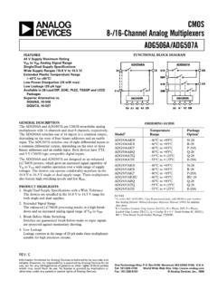
a 8-/16-Channel Analog Multiplexers CMOS …
www.analog.commultiplexers with 16 channels and dual 8 channels, respectively. The ADG506A switches one of 16 inputs to a common output, depending on the state of four binary addresses and an enable input. The ADG507A switches one of eight differential inputs to a common differential output, depending on the state of three binary addresses and an enable input.
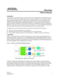
FPGA Architecture White Paper - Intel
www.intel.comSRAM bits to hold the configuration memory (CRAM) LUT-mask and a set of multiplexers to select the bit of CRAM that is to drive the output. To implement a k-input LUT (k-LUT)—a LUT that can implement any function of k inputs—2k SRAM bits and a 2k:1 multiplexer are needed. Figure 2 shows a 4-LUT, which consists of 16 bits of

Experiment # 7 Multiplexers And Demultiplexers
site.iugaza.edu.psMultiplexers: In electronics, a multiplexer (or mux) is a device that selects one of several analog or digital input signals and forwards the selected input into a single line. A multiplexer of 2n inputs has n select lines, which are used to select which input line

Optical Networks – Basic Concepts (Part 1)
www.iitg.ac.inAdddrop multiplexers using optical devices are called Optical Add/drop Multiplexers (OADM). Figure 10: An optical adddrop multiplexer (OADM) Optical Devices/components End nodes : sources or destinations of data (typically computers) . Optical routers : direct each incoming optical signal to an
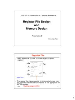
Register File Design and Memory Design
web.cse.ohio-state.eduThis is the RF design at the level of registers and multiplexers. Read regis ter numbe r 1 Read data 1 Read data 2 Read register number 2 Register file Write regi ster Write data Write 5 5 32 32 M u x R egi t r0 R gist r1 Registern–1 Registern M u x Re ad t 1 Re ad t 2 Readregister number1 R ead rgst number2 n=31 Figure B.8.8
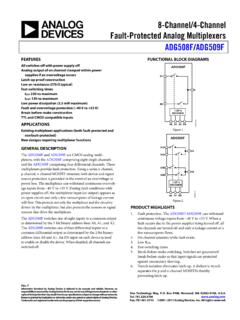
8-Channel/4-Channel Fault-Protected Analog Multiplexers ...
www.analog.commultiplexers provide fault protection. Using a series n-channel, p-channel, n-channel MOSFET structure, both device and signal source protection is provided in the event of an overvoltage or power loss. The multiplexer can withstand continuous overvolt-age inputs from −40 V to +55 V. During fault conditions with