
AN900 APPLICATION NOTE - STMicroelectronics
The resolution limit (minimal line size inside the circuit) of current technology is 0.35 microns. Achieving such results requires very sophisticated processes as well as superior quality levels. Backlap is the final step of wafer fabrication. The wafer thickness is reduced from 650 mi-
Download AN900 APPLICATION NOTE - STMicroelectronics

Information
Domain:
Source:
Link to this page:
Documents from same domain

Low-power dual operational amplifier - st.com
www.st.comFebruary 2016 DocID2471 Rev 17 1/24 This is information on a product in full production. www.st.com LM2904, LM2904A Low-power dual operational amplifier

AN3128 Application note - st.com
www.st.comJune 2011 Doc ID 16918 Rev 5 1/105 AN3128 Application note STM32 embedded graphic objects/touchscreen library Introduction This library is a firmware package which contains a collection of routines, data structures,

AN4767 Application note - st.com
www.st.comDocID028380 Rev 2 7/16 AN4767 Dual bank use cases 15 With dual bank, all the manipulation with the other bank is just another task of the main program.

AN3155 Application note - st.com
www.st.comOctober 2016 DocID17066 Rev 7 1/37 1 AN3155 Application note USART protocol used in the STM32 bootloader Introduction This application note describes the USART protocol used in the STM32 microcontroller

USB Power Delivery and Type-C - st.com
www.st.comUSB Type -C Overview USB Power Delivery specification introduces USB Type-C receptacle, plug and cable; they provide a smaller, thinner and more robust alternative to existing USB interconnect.

Datasheet - L78 - Positive voltage regulator ICs - …
www.st.comTO- 2 2 0 TO-2 2 0 F P DPAK D² PAK Features • Output current up to 1.5 A • Output voltages of 5; 6; 8; 8.5; 9; 12; 15; 18; 24 V • Thermal overload protection

AN2867 Application note - st.com
www.st.comMay 2017 DocID15287 Rev 11 1/43 1 AN2867 Application note Oscillator design guide for STM8AF/AL/S and STM32 microcontrollers Introduction Many designers know oscillators based on Pierce-Gate topology (hereinafter referred to as

AN4776 Application note - st.com
www.st.comMay 2017 DocID028459 Rev 2 1/73 1 AN4776 Application note General-purpose timer cookbook Introduction The timer peripheral is part of …

120-volt, 100-watt, DMOS audio amplifier with mute …
www.st.comSeptember 2010 Doc ID 6744 Rev 8 1/21 21 TDA7293 120-volt, 100-watt, DMOS audio amplifier with mute and standby Features Multipower BCD technology Very high operating voltage range (±50 V)

Electronic transformer for a 12V halogen lamp - …
www.st.comAPPLICATION NOTE AN528/0999 1/4 ELECTRONIC TRANSFORMER FOR A 12V HALOGEN LAMP by P. Fichera, R. Scollo 1. INTRODUCTION Lighting that uses halogen lamps is commonly found
Related documents

Sustainable Agriculture: An Introduction
s3.wp.wsu.eduUse Minimal Pesticides Prevent pest problems by building healthy, biologically active soil; by creat-ing habitat for beneficial organisms; and by choosing appropriate plant cultivars. View the farm as a component of an eco-system, and take actions to restore and enhance pest–predator balances. Under-stand that the mere presence of a pest

SPECIFICATION GUIDE SHEET for PASTURE AND HAY …
www.nrcs.usda.govNo-Till Drill – No-till seeding of forage crops can be used to replce rundown pastures and hayfields, to a supplement existing foage rsources, oreto r ... should be minimal. Weed competition can be minimized by careful use of sickle bar or rotary mowers.Clip the aea with r
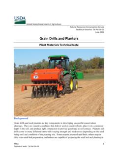
Grain Drills and Planters - USDA
www.nrcs.usda.govminimal change to the soil structure is desired. This minimal disturbance to the soil also reduces weed competition from early successional annual species that are set free by soil disturbances during typical seed bed preparation such as disking. Planting depth can be difficult to control with some no-till drills, especially with

s Guide to Agriculture Words, Terms and Definitions
extension.tennessee.eduand minimal disturbance of the soil. No-till is the most restrictive form of conservation tillage. Other practices or forms of minimum tillage would include ridge till, strip-till and mulch-till. Continuous Grazing: Refers to a grazing system where animals are left to graze in a eld for an extended period. Conventional Tillage/Seeding: Refers
Global agriculture towards 2050
www.fao.orgThe challenge Agriculture in the 21st century faces multiple challenges: it has to produce more food and fibre to feed a growing population with a smaller rural labour force, more

No-Till: The Quiet Revolution - USDA ARS
www.ars.usda.govidue. In contrast, no-till methods merely create in each planted row a groove just half an inch to three inches across into which seeds can be dropped, resulting in minimal overall soil dis-turbance. In the U.S., no-till agriculture fits under the broader U.S. Department of Agricul - ture definition of conservation tillage. Conser-

Ladda med rätt hagelpatron KUNDSKAPARNA Rätt ammunition
jagareforbundet.seFör att räknas till klass 2 måste kulan väga minst 3,2 g och värdet på E100 vara minst 800 J. Ammunition i klass 2 är tillåtet för allt vilt utom älg, hjort, vildsvin, björn, säl, mufflon, varg, visent och myskoxe. Klass 3 Kraven på ammunition i klass 3 är att kulan väger minst 2,5 g och har ett

Big plans get even bigger with minimal charges
www.hdfclife.comwith minimal charges* A Unit Linked Non-Participating Individual Life Insurance Plan Click 2 Wealth . Planning for future is one of the most important aspects of your life. May it be planning for your child’s future, ˜nancially securing your ... (till 99 years of age). You can opt for systematic withdrawal facility to generate recurring post