
Chapter 11 Differential Amplifier Circuits
The input voltage represented by common-mode voltage and differential voltage is shown in Fig. 11.2. Figure 11.2: Small differential and common-mode inputs of a differential amplifier Let V out1 be the output voltage due to input voltage V in1 and V out2 be the output voltage due to V in2. The differential-mode output voltage V out(d) be defined as
Download Chapter 11 Differential Amplifier Circuits

Information
Domain:
Source:
Link to this page:
Documents from same domain

Chapter 4 Junction Field Effect Transistor Theory …
staff.utar.edu.my4 Junction Field Effect Transistor Theory and Applications - 114 - Between point A and B, it is the ohmic region of the JFET. It is the region where the voltage and current relationship follows ohm's law.

Chapter 16 Oscillator Circuits and Applications
staff.utar.edu.mywhere A V is the voltage gain of the amplifier and β = V Vout f is the feedback ... Many oscillators are designed utilizing RC network and resistor divider circuits. RC network is basically used to determine the resonant frequency of the oscillator, whilst resistor divider circuit is used to provide attenuated feedback. ...
Chapter 9 Design of Counters - Universiti Tunku Abdul Rahman
staff.utar.edu.my09 Design of Counters - 116 - Based on the results obtained from the Karnaugh maps, the circuit design of synchronous decade counter is shown in Fig. 9.15. Figure 9.15: A synchronous decade counter designed using JK flip-flop 9.4.2 Design of an …

Chapter 5 Physics of MOSFET and MOSFET Modeling
staff.utar.edu.my5 Physics of MOSFET and MOSFET Modeling - 88 - where N A is the acceptor doping concentration for p-type semiconductor, ni is the intrinsic carrier concentration and kT/q is the thermal voltage. Substituting equation (5.2) into equation (5.1) yields equation (5.3).

Chapter 16 Fourier Series Analysis
staff.utar.edu.myA rectified half sine wave is defined over one period f(t) = Asin ωt for 0 < t < T/2 and f(t) = 0 for T/2 < t < T as shown in Fig. 16.1. Find the Fourier series of this wave form. Figure 16.1: A half-wave rectifier Solution The dc voltage shall be a 0 = ∫ ω + ∫ T T / 2 T / 2 0 0dt T 1 Asin tdt T 1 = π = − ω ω − A 1 2 T cos T A. The
Related documents

AD8131 Low Cost, High Speed Differential Driver Data Sheet ...
www.analog.comThe AD8131’s differential output also helps balance the input for differential ADCs, optimizing the distortion performance of the ADCs. The common-mode level of the differential output is adjustable by a voltage on the V OCM pin, easily level-shifting the input signals for driving single-supply ADCs with dual supply signals.

MT-041: Op Amp Input and Output Common-Mode and ...
www.analog.comDifferential Voltage Range . INPUT AND OUTPUT VOLTAGE RANGE . Some practical basic points are now considered regarding the allowable input and output voltage ranges of a real op amp. This obviously varies with not only the specific device, but also the supply voltage. While we can always optimize this performance point with device selection,
Basic Amplifiers and Differential Amplifier
www.cse.psu.edu− Voltage Gain (ex. >30) − Active Common Mode Input range (as large as possible) − Others: slew rate, CMRR, PSRR, etc. Determine minimum channel length 2/22/2011 Insoo Kim Determine channel width − Determine W 1,2 from voltage gain spec. − Determine W 5 & Bias Voltagefrom power consumption & CM min. − Determine W 3,4 from CM max.
A Test Bench for Differential Circuits
designers-guide.orgTo measure differential-mode gain using an AC analysis, set the AC magnitude on Vid to 1 V and on all other sources to 0. For simpli city, assume that this is a low frequency application and both Rid and Ric are 0 Ω. Perform the AC analysis. Then the differential voltage gain is identical to the voltage at the d terminal of Bo (because the ...
APPLICATIONS OF SECOND-ORDER DIFFERENTIAL …
www.math.pitt.eduIn Additional Topics: Linear Differential Equationswe were able to use first-order linear equations to analyze electric circuits that contain a resistor and inductor. Now that ... It is known from physics that the voltage drops across the resistor, induc-tor, and capacitor are
Differential and Common Mode Gain lecture - ITTC
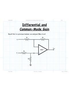
www.ittc.ku.edu2/18/2011 Differential and Common Mode Gain lecture 6/8 Jim Stiles The Univ. of Kansas Dept. of EECS Difference amplifiers should have no common-mode gain Note that each of these gains are open-circuit voltage gains. * An ideal differential amplifier …

LECTURE 19 DIFFERENTIAL AMPLIFIER - AICDESIGN.ORG
aicdesign.orginput voltage in favor of the differential-input voltage. • Input common-mode range (ICMR) The input common-mode range is the range of common-mode voltages over which the differential amplifier continues to sense and amplify the difference signal with the same gain. Typically, the ICMR is defined by the common-mode voltage range over which all
Differential Amplifier Stages - MIT OpenCourseWare
ocw.mit.eduDifferential Amplifier Stages - Large signal behavior General features: symmetry, inputs, outputs, biasing (Symmetry is the key!) Large signal transfer characteristic . Difference- and common-mode signals. Decomposing and reconstructing general signals . Half-circuit incremental analysis techniques. Linear equivalent half-circuits

Differential Clock Translation - Microchip Technology
ww1.microchip.comLow-Voltage, Positive-Referenced, Emitter-Coupled Logic (LVPECL) Low-voltage, positivereferenced, emitter- -coupled logic (LVPECL) originates from -coupled logic (emitter ECL), adopting a positive power supply. The LVPECL input is a current-switching differential pair with high input impedance(see . Figure 1 . The input )