
DESIGNING SEQUENTIAL LOGIC CIRCUITS
7.9 Non-Bistable Sequential Circuits 7.9.1The Schmitt Trigger 7.9.2Monostable Sequential Circuits 7.9.3Astable Circuits 7.10 Perspective: Choosing a Clocking Strategy 7.11 Summary 7.12 To Probe Further 7.13 Exercises and Design Problems chapter7_pub.fm Page …
Download DESIGNING SEQUENTIAL LOGIC CIRCUITS

Information
Domain:
Source:
Link to this page:
Documents from same domain
chapter2.fm Page 33 Monday, September 4, 2000 …
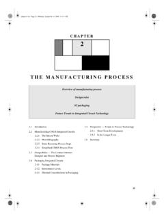
bwrcs.eecs.berkeley.eduIC packaging Future Trends in Integrated Circuit Technology 2.1 Introduction 2.2 Manufacturing CMOS Integrated Circuits 2.2.1 The Silicon Wafer 2.2.2 Photolithography 2.2.3 Some Recurring Process Steps ... cess that lies at the core of the semiconductor revolution. Yet, some insight in the steps ...

Designing a Divider - University of California, Berkeley
bwrcs.eecs.berkeley.eduDigital Integrated Circuits 2/e DIVIDE HARDWARE Version 1 ° 64-bit Divisor reg, 64-bit ALU, 64-bit Remainder reg, 32-bit Quotient reg Remainder Quotient Divisor …
CMOS Manufacturing Process
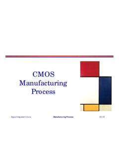
bwrcs.eecs.berkeley.eduDigital Integrated Circuits Manufacturing Process EE141 A Modern CMOS Process p-well n-well p+ p-epi SiO 2 AlCu poly n+ SiO 2 p+ gate-oxide Tungsten TiSi 2 Dual-Well Trench-Isolated CMOS Process
Lecture 9: Digital Signal Processors: Applications and ...
bwrcs.eecs.berkeley.eduProcessor Applications General Purpose - high performance ... Digital camera - TMS320C5000 ... DSP evolved from Analog Signal Processors, using analog hardware to transform phyical signals (classical electrical engineering) ASP to DSP because

DESIGNING COMBINATIONAL LOGIC GATES IN CMOS
bwrcs.eecs.berkeley.edu198 DESIGNING COMBINATIONAL LOGIC GATES IN CMOS Chapter 6 6.1Introduction The design considerations for a simple inverter circuit ere presented in the previousw chapter. In this chapter, the design of the inverter will be extended to address the synthesis

Lecture11-MOS Cap Delay
bwrcs.eecs.berkeley.eduEE141 25 EECS141 Lecture #11 25 The Miller Effect V in M1 C gd1 V out ∆V As V in increases, V out drops – Once get into the transition region, gain from V in to V out > 1 So, C gd experiences voltage swing larger than V
Chapter 4 Calculating the Logical Effort of Gates
bwrcs.eecs.berkeley.edu4.3 Calculating logical effort Definition 4.2 provides a convenient method for calculating the logical effort of a logic gate. We have but to design a gate that has the same current drive character-istics as a reference inverter, calculate the input capacitances of each signal, and apply Equation 4.1 to obtain the logical effort.

DESIGNING COMBINATIONAL LOGIC GATES IN CMOS
bwrcs.eecs.berkeley.eduof arbitrary digital gates such as NOR, NAND and XOR. The focus will be on combina-tional logic (or non-regenerative) circuits that have the property that at any point in time, the output of the circuit is related to its current input signals by some Boolean expression (assuming that the transients through the logic gates have settled).
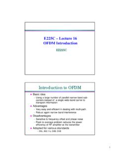
Introduction to OFDM
bwrcs.eecs.berkeley.eduOFDM Introduction EE225C Introduction to OFDM lBasic idea ... – Selective Fading – Very short pulses – ISI iscompartively long – EQs are then very long – Poor spectral efficiency because of band guards Drawbacks ... 2 4 6 8 10 12 14 16-60-55-50-45-40-35-30-25-20-15-10

SEMICONDUCTOR MEMORIES
bwrcs.eecs.berkeley.eduThe read-out of the 1T DRAM cell is destructive; read and refresh operations are necessary for correct operation. Unlike 3T cell, 1T cell requires presence of an extra capacitance that must be explicitly included in the design. When writing a “1” into a DRAM cell, a threshold voltage is lost.
Related documents

Basic Networking Concepts - UVic.ca
www.ece.uvic.caelectronic circuits for data transmission etc. Data link layer: in charge of data encapsulation under the form of packets and their interpretation at the physical layer. Network layer: in charge of packets transmission from a source A to a destination B. Transport layer: in charge of the delivery of packets from a source A to a destination B

Transmission Line Equations - Amanogawa
amanogawa.comTransmission Lines © Amanogawa, 2006 – Digital Maestro Series 41 If you are only familiar with low frequency circuits, you are used to treat all lines connecting ...
CONSTRUCTION STANDARDS STANDARD DRAWINGS - WAPA
www.wapa.gov114. 41 6157 – Standard Design Transmission Lines Type 3TD 115Kv 3-pole Tension Dead End Structure 115. 41 9002 Rev. N – Transmission Line Standards Barbed Wire Gate For Right -of-Way Fences 116. 41 9003 Rev. C – Transmission Line Standards Electric Barbed Wire Gate For Right -of-Way Fences
ChapterII RF-CIRCUITS - DTU
rftoolbox.dtu.dkQ circuits too.1 For obvious reasons such circuits are also called narrowbanded. Fig.5 Normalized magnitudes and phases in the impedance of parallel tuned circuits with varying Q-factors. PolesandZeros Pole and zero positions are useful for investigating responses of frequency selective networks that include parallel tuned circuits.