Introduction to Bluetooth Device Testing - NI
Figure 4. Location of RF Physical Layer in Bluetooth Protocol Stack. This section will cover operating frequencies, modulation, and frequency hopping, transmit power, and receiver power. First, the channel arrangement topic discusses spacing between channels and the number of channels that are used.
Download Introduction to Bluetooth Device Testing - NI

Information
Domain:
Source:
Link to this page:
Documents from same domain
Controller Area Network (CAN) Tutorial - National …
download.ni.com©National Instruments Corporation 1-1 Controller Area Network (CAN) Tutorial Controller Area Network (CAN) Tutorial A Controller Area Network (CAN) bus is a high-integrity serial bus system

TR TECHNICAL REPORT ELPEGUARD
download.ni.comTechnical Report of the series ELPEGUARDfi SL 1307 2 www.peters.de 1. General information The conformal coatings of the series ELPEGUARDfi SL 1307 are …

Flexible Manufacturing With Time Sensitive …
download.ni.comFlexible Manufacturing With Time Sensitive Networking An NI Industrial IoT Lab Demonstration Time Sensitive Networking (TSN) is a set of new capabilities being added to the IEEE Ethernet standards.

Understanding FFTs and Windowing
download.ni.comni.com/instrument-fundamentals Next Understanding FFTs and Windowing Overview Learn about the time and frequency domain, fast Fourier transforms (FFTs), and
Introduction to LabVIEW - National Instruments
download.ni.comIntroduction to LabVIEW 1. Introduction Welcome to the LabVIEW component of EE100! This lab is just a simple introduction to the graphical circuit simulation ...

Archived: Getting Started: PXI 8211 for Windows - National ...
download.ni.comThe installation guide also contains cabling instructions and troubleshooting tips. 4. 1 Shut down, then power off computer. 2 Install hardware and cables, then power on computer. ... Archived: Getting Started: PXI 8211 for Windows - National Instruments Author: Technical Communications

NI USB-9213 User Guide and Specifications - National ...
download.ni.comUSB Devices Getting Started Guide that shipped with your device, and is also accessible from Start»All Programs»National Instruments» NI-DAQ , for more information.

The Engineer’s Guide to Signal Conditioning
download.ni.commeasurement to obtain the true temperature. This adjustment is known as cold junction compensation (CJC). Most thermocouple measurement devices include built-in CJC and automatic scaling in software. If the data acquisition device does not have built-in CJC, the temperature must be measured externally to account for this difference in software.

Lab 1 – Wheatstone Bridge
download.ni.comthe potential difference between V1 and V2. The voltage gain of the differential amplifier is giving by the ratio 4 3 R R or by 6 5 R R Since the voltage gain should be 1, then R3 = R5 and R4 = R6. This can be easily accomplished by selecting R4 = R6 = 1 kΩ and R3 = R5 = 1 kΩ. U4 is an amplifier with gain of 2.2 according to the problem ...
Declaration of Conformity
download.ni.comRoHS Directive (EU) 2015/863 amending Annex II to Directive 2011/65/EU Conformity is assessed in accordance to the following standards: September 15, 2020, Austin, Texas USA Date and Place of Issue Dany Cheij, Global Product & Trade Compliance Manager
Related documents
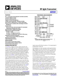
RF Agile Transceiver Data Sheet AD9361 - Analog Devices
www.analog.comThe AD9361 is a high performance, highly integrated radio frequency (RF) Agile Transceiver™ designed for use in 3G and 4G base station applications. Its programmability and wideband capability make it ideal for a broad range of transceiver applications. The device combines a RF front end with a flexible mixed-signal
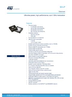
Datasheet - S2-LP - Ultra-low power, high performance, sub ...
www.st.comThe S2-LP is a high performance ultra-low power RF transceiver, intended for RF wireless applications in the sub-1 GHz band. It is designed to operate in both the license-free ISM and SRD frequency bands at 433, 512, 868 and 920 MHz, but can also be programmed to operate at other additional frequencies in the 413-479 MHz,

ALL MODE MULTI-BAND TRANSCEIVER TS-2000 TS-2000X …
www.kenwood.com• Disconnect the input power cable from the power source when the transceiver is not used for long periods of time. • Remove the transceiver’s enclosure only to do accessory installations described in this manual or accessory manuals. Follow provided instructions carefully, to avoid electrical shocks. If unfamiliar

RF Basics, RF for Non-RF Engineers - Texas Instruments
www.ti.comTransceiver System-on-Chip ... No extra signal is needed from MCU to turn off LNA in low power modes RF_P TXRX_SWITCH RF_N CC2420 BALUN TX/RX Switch ANT PA LP filter TX path RX path Control logic and bias network RX current 19.7 mA 19.7 mA Line of 230 meter 580 meter Sight Range Sensitivity -94 dBm -93.1 dBm
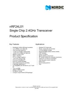
nRF24L01 Product Specification V2 - SparkFun Electronics
cdn.sparkfun.com11 VDD_PA Power Output Power Supply Output(+1.8V) for the internal nRF24L01 Power Amplifier. Must be con-nected to ANT1 and ANT2 as shown in Fig-ure 30. 12 ANT1 RF Antenna interface 1 13 ANT2 RF Antenna interface 2 14 VSS Power Ground (0V) 15 VDD Power Power Supply (+1.9V - +3.6V DC) 16 IREF Analog Input Reference current. Connect a 22kΩ ...

RF Agile Transceiver Data Sheet AD9363 - Analog Devices
www.analog.comThe AD9363 is a high performance, highly integrated RF agile transceiver designed for use in 3G and 4G femtocell applications. Its programmability a nd wideband capability make it ideal for a broad rang e of transceiver applications. Th e device combines an RF front end with a flexible mixed-signal baseband section and