
Lecture11-MOS Cap Delay
Capacitance [arbitrary units] N+ junction area N+ junction perimeter P+ junction area P+ junction perimeter Junction caps are nonlinear –C J is a function of junction bias EE141 18 EECS141 Lecture #11 18 Linearizing the Junction Capacitance Replace non-linear capacitance by large-signal equivalent linear capacitance
Download Lecture11-MOS Cap Delay

Information
Domain:
Source:
Link to this page:
Documents from same domain
chapter2.fm Page 33 Monday, September 4, 2000 …
bwrcs.eecs.berkeley.eduIC packaging Future Trends in Integrated Circuit Technology 2.1 Introduction 2.2 Manufacturing CMOS Integrated Circuits 2.2.1 The Silicon Wafer 2.2.2 Photolithography 2.2.3 Some Recurring Process Steps ... cess that lies at the core of the semiconductor revolution. Yet, some insight in the steps ...

Designing a Divider - University of California, Berkeley
bwrcs.eecs.berkeley.eduDigital Integrated Circuits 2/e DIVIDE HARDWARE Version 1 ° 64-bit Divisor reg, 64-bit ALU, 64-bit Remainder reg, 32-bit Quotient reg Remainder Quotient Divisor …
CMOS Manufacturing Process
bwrcs.eecs.berkeley.eduDigital Integrated Circuits Manufacturing Process EE141 A Modern CMOS Process p-well n-well p+ p-epi SiO 2 AlCu poly n+ SiO 2 p+ gate-oxide Tungsten TiSi 2 Dual-Well Trench-Isolated CMOS Process
Lecture 9: Digital Signal Processors: Applications and ...
bwrcs.eecs.berkeley.eduProcessor Applications General Purpose - high performance ... Digital camera - TMS320C5000 ... DSP evolved from Analog Signal Processors, using analog hardware to transform phyical signals (classical electrical engineering) ASP to DSP because

DESIGNING COMBINATIONAL LOGIC GATES IN CMOS
bwrcs.eecs.berkeley.edu198 DESIGNING COMBINATIONAL LOGIC GATES IN CMOS Chapter 6 6.1Introduction The design considerations for a simple inverter circuit ere presented in the previousw chapter. In this chapter, the design of the inverter will be extended to address the synthesis

DESIGNING SEQUENTIAL LOGIC CIRCUITS
bwrcs.eecs.berkeley.edu272 DESIGNING SEQUENTIAL LOGIC CIRCUITS Chapter 7 7.1 Introduction Combinational logic circuits that were described earlier have the property that the output
Chapter 4 Calculating the Logical Effort of Gates
bwrcs.eecs.berkeley.edu4.3 Calculating logical effort Definition 4.2 provides a convenient method for calculating the logical effort of a logic gate. We have but to design a gate that has the same current drive character-istics as a reference inverter, calculate the input capacitances of each signal, and apply Equation 4.1 to obtain the logical effort.

DESIGNING COMBINATIONAL LOGIC GATES IN CMOS
bwrcs.eecs.berkeley.eduof arbitrary digital gates such as NOR, NAND and XOR. The focus will be on combina-tional logic (or non-regenerative) circuits that have the property that at any point in time, the output of the circuit is related to its current input signals by some Boolean expression (assuming that the transients through the logic gates have settled).
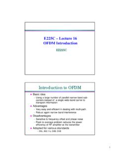
Introduction to OFDM
bwrcs.eecs.berkeley.eduOFDM Introduction EE225C Introduction to OFDM lBasic idea ... – Selective Fading – Very short pulses – ISI iscompartively long – EQs are then very long – Poor spectral efficiency because of band guards Drawbacks ... 2 4 6 8 10 12 14 16-60-55-50-45-40-35-30-25-20-15-10

SEMICONDUCTOR MEMORIES
bwrcs.eecs.berkeley.eduThe read-out of the 1T DRAM cell is destructive; read and refresh operations are necessary for correct operation. Unlike 3T cell, 1T cell requires presence of an extra capacitance that must be explicitly included in the design. When writing a “1” into a DRAM cell, a threshold voltage is lost.
Related documents
Experiment 8: Capacitance and the Oscilloscope
www.columbia.eduPHYS 1493/1494/2699: Exp. 8 – Capacitance and the oscilloscope 2 Outline Capacitance: − Capacitor as a charge storage device − Capacitors in combination − RC circuits: exponential growth and decay Oscilloscope: − Conversion of analog signals to digital − Display and signal operations Measurements: − Large RC charging − Large RC discharging

CMOS Capacitance and Circuit Delay
inst.eecs.berkeley.eduCapacitance CSD has a bottom and out-side perimeter between the source or drain and the underlying substrate which is connected to a.c. ground. There is also a gate perimeter component for which there is a 2X magnifying (Miller) effect on the S/D side because the

2. Features and benefits PRTR5V0U2X - Nexperia
assets.nexperia.comUltra low capacitance double rail-to-rail ESD protection diode 10. Application information Handling data rates up to 480 Mbit/s, USB 2.0 interfaces require ESD protection devices with an extremely low line capacitance in order to avoid signal distortion. With a capacitance of only 1 pF, the device offers IEC 61000-4-2, level 4 compliant ESD ...

ECE 340 Lecture 27 : Junction Capacitance
transport.ece.illinois.eduJunction Capacitance When combine the equations result in the charge on either side of the dipole… Total charge: v Clearly a non-linear function of the applied voltage. Now apply the definition of the capacitance… Junction Capacitance: v •The junction capacitance is a voltage-variable capacitance.

Chapter 5 Capacitance and Dielectrics
web.mit.eduCapacitance and Dielectrics 5.1 Introduction A capacitor is a device which stores electric charge. Capacitors vary in shape and size, but the basic configuration is two conductors carrying equal but opposite charges (Figure

Depletion Capacitance - University of California, Berkeley
inst.eecs.berkeley.eduEE 105 Fall 2000 Page 2 Week 4 Depletion Capacitance (cont.) n break up the charge qJ on the p-side of the junction similarly: total charge in the depletion region = DC charge + small-signal charge qJ = Q J + qj note that the DC charge is a negative number
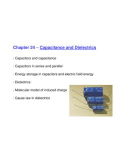
Chapter 24 – Capacitance and Dielectrics
physics.ucf.edu- Capacitance is a measurement of the ability of capacitor to store energy (V = U / q). Capacitors in Vacuum - Parallel Plate Capacitor: uniform electric field between the plates, charge uniformly distributed over opposite surfaces A Q E εo εo σ = = d A V Q C ab = =ε0 A Qd V E d o ab ε 1 = ⋅ = ε0 = 8.85 x 10⁻¹² F/m

AP Physics Practice Test: Capacitance, Resistance, DC Circuits
www.crashwhite.comCapacitance, Resistance, DC Circuits ©2013, Richard White www.crashwhite.com 4. Three capacitors, of capacitance 1µF, 5µF, and 6µF, are arranged in a circuit with a switch and a 12-V battery as shown above. The equivalent capacitance of the three capacitors is: a. 2 µF b. 3 µF c. 6 µF d. 11/6 µF e. 11/12 µF 5. Two conducting wires, W 1 ...

Chapter Two ELECTROSTATIC POTENTIAL AND …
www.ncert.nic.inand Capacitance 2.3 Figure 2.2 shows some equipotential lines distributed in space. A charged object is moved from point A to point B. (a) The work done in Fig. (i) is the greatest. (b) The work done in Fig. (ii) is least. (c) The work done is the same in Fig. (i), Fig. (ii) and Fig. (iii).