
Microelectronics Reliability: Physics-of-Failure Based ...
functionality, decrease costs, and reduce design and development time. As a result, device feature ... CMOS Complementary Metal Oxide Semiconductor COTS Commercial-off-the-Shelf DAC Digital-to-Analog Converter ... VLSI Very Large Scale Integration . ix
Download Microelectronics Reliability: Physics-of-Failure Based ...

Information
Domain:
Source:
Link to this page:
Documents from same domain
Photonic Integrated Circuit (PIC) Device Structures ...
nepp.nasa.govand construct electronic devices onto a single CMOS chip. Photonic integrated circuits (PICs) exist as the optical analog to integrated circuits; however, in place of transistors, PICs consist of numerous scaled

Assessing and Mitigating Radiation Effects in Xilinx FPGAs
nepp.nasa.govThis research was carried out at the Jet Propulsion Laboratory, California Institute of Technology, and was sponsored by the National Aeronautics and Space Administration Electronic Parts and Packaging (NEPP) Program.

Radiation Effects Assessment of MRAM Devices - NASA
nepp.nasa.govRadiation Effects Assessment of MRAM Devices Mohamed Elghefari Jet Propulsion Laboratory Pasadena, California Steve McClure Jet Propulsion Laboratory Pasadena, California Jet Propulsion Laboratory California Institute of Technology Pasadena, California JPL Publication 08-19 5/08 .

S-311-S-819 - Resistor, Fixed, Foil (Managanin) Power ...
nepp.nasa.govSurface Mount CODE 311 SUPERVISORY APPROV~: I I I Ronald Chinnapongse ~~ Ir~7 ... fOil, precIsion, current sensing resistor In a surface mounted package. This 4-terminal (two power J-shaped and two sense gull-wing-shaped) resistor is intended for use in ... Marking shall in no way interfere with or obscure any of the original manufacturer's ...

S-311-S-821 - Resistor, Fixed, Foil (Manganin), Chip ...
nepp.nasa.govfOil, precIsion, current sensing resistor In a surface mounted package. This chip ... Marking shall in no way interfere with or obscure any of the original manufacturer's marking. b. The number of lines shall be at discretion of the test facility or laboratory. ... Foil (Manganin), Chip, Power, Current Sensing, Surface Mount ...

Mechanical Properties and Microstructure Investigation Of ...
nepp.nasa.govSn-Ag-Cu alloy is considered the preferred substitute for tin-lead solder in reflow applications due to its relatively low melting temperature, and superior mechanical properties and solderability compared with other lead free solders.

32 IEEE TRANSACTIONS ON ELECTRONICS PACKAGING ...
nepp.nasa.govCOUREY et al.: TIN WHISKER ELECTRICAL SHORT CIRCUIT CHARACTERISTICS—PART I 33 considers the following factors: conductor spacing, lead con-tent in tin plating, process by which the tin was deposited, tin thickness, materialdirectly beneaththetin, substrate controlling
IEEE TRANSACTIONS ON ELECTRONICS PACKAGING …
nepp.nasa.govCOUREY et al.: TIN WHISKER ELECTRICAL SHORT CIRCUIT CHARACTERISTICS—PART II 43 Fig. 4. Schematic diagram for the tin whisker test station instrumentation. Re-produced from [4]. Fig. 5. Tin whisker test station probing area close up.
Temperature Dependent Dielectric Properties of ...
nepp.nasa.govTemperature Dependent Dielectric Properties of Polycrystalline 96%Al 2O 3 Liang-Yu Chen1 and Gary W. Hunter2 1Ohio Aerospace Institute/NASA Glenn Research Center at Lewis Field, Cleveland, OH 44135 2NASA Glenn Research Center at Lewis Field, Cleveland, OH 44135 Abstract Polycrystalline Al 2O 3 substrates have been proposed and tested for high ...

Space Grade Requirements for Electrical Connectors
nepp.nasa.govGSFC-S-311-P-10, Subminiature, electrical and coaxial contact, electrical, connector. Military Specifications and Standards MIL-STD-1344 Test Methods for Electrical Connectors MIL-STD-202: Test Methods for Electronic and Electrical Component parts MIL-C-5015, Circular, threaded, AN type, electrical, connector.
Related documents
Behavioral Modeling using Verilog-A
lumerink.comPowerful method for complex design verification Language construct is similar to digital Verilog RTL, but not quite the same Easy to pick up, but mastery comes with experience Can be used to model novel devices not covered by bsim

CMOS Technology and Logic Gates - MIT OpenCourseWare
ocw.mit.eduCMOS VLSI is thedigital implementation technology of choice for the foreseeable future (next 10-20 years) – Excellent energy versus delay characteristics – High density of wires and transistors – Monolithic manufacturing of devices and interconnect, cheap! 6.884 – Spring 2005 2/07/2005 L03 – CMOS Technology 4

Sigma-Delta ADCs and DACs - CCRMA
ccrma.stanford.edumixed-signal VLSI processes. Until recently, however, the process technology needed to make these devices commercially viable has not been available. Now that 1 micron and smaller CMOS geometries are manufacture able, sigma-delta converters will become even more prolific in certain types of applications, especially mixed-signal ICs which combine

5. CMOS Operational Amplifiers - IMS
ims.unipv.itAnalog Design for CMOS VLSI Systems Franco Maloberti Input offset voltage: In real circuits if the two input terminals are set at the same voltage the output saturates close to VDD or to VSS. Input common mode range: It is the maximum range of the common-mode input voltage which do not produce a significant variation of the differential gain.
Introduction to Analog Layout Design - SMDP-C2SD
smdpc2sd.gov.in• Typically Analog is 20% and digital 80% of the chip area. – Analog requires 80% of the design time • Requires more iterations –Passes for success: 2-3 for analog, 1 for digital. • In general, analog circuits are more complex than digital. – Need to have good knowledge of both circuit analysis, modeling and technology Analog VLSI ...
Chapter 16.1 NMOS Inverter - Introduction to VLSI
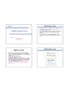
ece424.cankaya.edu.trCMOS The most abundant devices on earth ¾Although the processing is more complicated for CMOS circuits than for NMOS circuits, CMOS has replaced NMOS at all level of integration, in both analog and digital applications. ¾The basic reason of this replacement is that the power dissipation in CMOS logic circuits is much less than in NMOS circuits.

VLSI Design Lecture PPTs
www.iare.ac.inVLSI Design Lecture PPTs INSTITUTE OF AERONAUTICAL ENGINEERING Dundigal, Hyderabad -500 043 6/3/2015 1 Department : ELECTRONICS AND COMMUNICATION ENGINEERING Course Code : 57035 Course Title : VLSI DESIGN Course Coordinator : VR. Sheshagiri Rao, Professor Team of Instructors B. Kiran Kumar , Assistant Professor Course …