
Preliminary Product Specification v1
7 VDD Power Power Supply (+1.9V - +3.6V DC) 8 VSS Power Ground (0V) 9 XC2 Analog Output Crystal Pin 2 10 XC1 Analog Input Crystal Pin 1 11 VDD_PA Power Output Power Supply Output (+1.8V) for the internal nRF24L01+ Power Amplifier. Must …
Download Preliminary Product Specification v1

Information
Domain:
Source:
Link to this page:
Documents from same domain

AT Commands Reference Guide - SparkFun …
www.sparkfun.comAT Commands Reference Guide 80000ST10025a Rev. 0 - 04/08/06 Reproduction forbidden without Telit Communications S.p.A. written authorization - All …
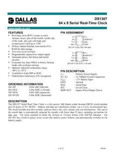
DS1307 64 x 8 Serial Real-Time Clock
www.sparkfun.com1 of 12 100101 FEATURES Real-time clock (RTC) counts seconds, minutes, hours, date of the month, month, day of the week, and year with …

Advanced User Manual - SparkFun Electronics
www.sparkfun.comusage information and a summary of common commands refer to the Install Guide for a given product. Version 4.77 August 27, 2009 Roving Networks reserves the right to make corrections, modifications, and changes to its products, documentation and services ... Advanced User Manual.

Single chip 2.4 GHz Transceiver nRF24L01
www.sparkfun.comPRELIMINARY PRODUCT SPECIFICATION nRF24L01 Single Chip 2.4 GHz Radio Transceiver Nordic Semiconductor ASA - Vestre Rosten 81, N-7075 Tiller, Norway - Phone +4772898900 - …

XBee /XBee-PRO RF Modules - SparkFun Electronics
www.sparkfun.comThe XBee®/XBee-PRO® RF Module was designed to mount into a receptacle (socket) and there-fore does not require any soldering when mounting it to a board. The XBee Development Kits con-tain RS-232 and USB interface boards which use two 20-pin receptacles to receive modules.

GSM/GPRS Module - SparkFun Electronics
www.sparkfun.comThis document gives an overview of the LinkSprite GSM/GPRS module: a miniature, single-side board, quad-band GSM 850/EGSM 900/DCS 1800/PCS 1900 module, ready for integration in various kinds of Fix wireless phones and other wireless devices.

16-Channel Constant-Current LED Driver
www.sparkfun.comA6282 Description The A6282 device is designed for LED display applications. This CMOS device includes an input shift register, accompanying data latches, and 16 MOS constant current sink drivers.

+3.3V Low Power Half-Duplex RS-485 Transceivers with ...
www.sparkfun.com10/15/02 SP3481/3485 Low Power Half-Duplex RS485 Transceivers © Copyright 2000 Sipex Corporation 2 SPECIFICATIONS T AMB = T MIN to T MAX and V CC = +3.3V ± 5% ...
XBee /XBee-PRO RF Modules - SparkFun Electronics
www.sparkfun.comDigi International Inc. 11001 Bren Road East Minnetonka, MN 55343 877 912-3444 or 952 912-3444 http://www.digi.com XBee®/XBee-PRO® RF Modules XBee®/XBee-PRO® RF ...

Typical Application - sparkfun.com
www.sparkfun.comFully Integrated, Hall Effect-Based Linear Current Sensor with ACS712 2.1 kVRMS Voltage Isolation and a Low-Resistance Current Conductor Allegro MicroSystems, Inc. 3 115 Northeast Cutoff
Related documents

USB 3.0 Hub Controller
jfd-ic.comThe purpose of this document is to provide suggestions for the design of circuit and PCB layout regarding the USB 3.0 Hub Controllers of Genesys Logic Inc. 2. CIRCUIT DESIGN AND PCB LAYOUT GUIDELINES 2.1 AC Coupling Capacitors PHY is a component where the transmitter and receiver are located and operated together. The AC coupling
nRF24L01 Product Specification V2 - SparkFun Electronics
cdn.sparkfun.com7 VDD Power Power Supply (+1.9V - +3.6V DC) 8 VSS Power Ground (0V) 9 XC2 Analog Output Crystal Pin 2 10 XC1 Analog Input Crystal Pin 1 11 VDD_PA Power Output Power Supply Output(+1.8V) for the internal nRF24L01 Power Amplifier. Must be con-nected to ANT1 and ANT2 as shown in Fig-ure 30. 12 ANT1 RF Antenna interface 1 13 ANT2 RF Antenna interface 2

Programming Guide VLT Midi Drive FC 280
files.danfoss.comturn power on again. Power factor The power factor is the relation between I1 and IRMS. Power factor = 3 x U x I 1 cos ϕ1 3 x U x I RMS cosϕ1 = 1, therefore: Power factor = I 1 x cos ϕ1 I RMS = I 1 I RMS The power factor indicates to which extent the frequency converter imposes a load on the mains supply.
DDR2, DDR3, and DDR4 SDRAM Board Design Guidelines 4
www.intel.co.jp• Layout guidelines As memory interface performance increases, board designers must pay closer attention to the quality of the ... Controllers must compensate for this skew by adjusting the timing per byte lane. During a write, DQS groups launch at separate times to coincide with a clock arriving at components on ... power-up or when the DDR3 ...

AN1131 Layout Guide - Silicon Labs
www.skyworksinc.com7.1 Adding Capacitance Between Power Domains. 23. 7.2 Using Common-Mode Chokes to Reduce Emissions. 25. 8. Controlling Emissions in Designs using Digital Isolators with Integrated DC-DC Controllers. 27. 8.1 Primary-Side Loop Currents. 28. 8.2 Secondary-side Loop Currents. 28. 8.3 Using Secondary-Side Snubber Circuit to Reduce Emissions Due to ...