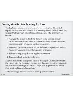
Solving circuits directly using Laplace
voltage divider. = 1 sC R+ 1 sC +sL V i (s) V C (s) = Z C Z R +Z C +Z L V i (s) V C (s) = (1 1+sRC+s2LC)(V f s) = V f LC s(s2 +s R L + 1 LC) – + + – Z R V i (s) Z C V C (s) Z L Convert to the frequency domain. Z R = R
Download Solving circuits directly using Laplace

Information
Domain:
Source:
Link to this page:
Documents from same domain
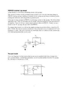
pspice op amp - Iowa State University
tuttle.merc.iastate.eduThis tutorial is written with the assumption that you know how to do ... So it looks like the uA741 model has the potential to be a reasonably accurate PSPICE op amp

How Millennials Can Get Rich Slowly
tuttle.merc.iastate.eduHow Millennials Can Get Rich Slowly William J. Bernstein ©2014 . Would you believe me if I told you that there’s an investment strategy that a seven-year-old could ... and vigor, your retirement options may well range between moving in with your kids and sleeping under a bridge in the rain.

First-order filters - Iowa State University
tuttle.merc.iastate.eduFirst-order filters The general form for the transfer function of a first order filter is: T(s) = G o ... Use the standard definition for cut-off frequency, which is the frequency at which the magnitude is down by from the value in the pass-band. For our low-pass function, the pass band is at low frequencies, and the ...

Basic PMOS structure - Iowa State University
tuttle.merc.iastate.eduohmic or linear v GS < V T v DS < v GS – V T i D = K[v GS – V T]2 saturation Summary of PMOS equations K = 1 2 μCox W L VT < 0 Note the equations are identical to the NMOS equations. For a PMOS, v GS and v DS are both negative and the current flows from source to drain.
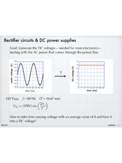
Rectifier circuits & DC power supplies
tuttle.merc.iastate.eduNov 01, 2015 · Rectifier circuits & DC power supplies Goal: Generate the DC voltages – needed for most electronics – starting with the AC power that comes through the power line.? 120 V RMS 9DF=( 9)sin 7 W f = 60 Hz (T = 16.67 ms) How to take time-varying voltage with an average value of 0 and turn it into a DC voltage?
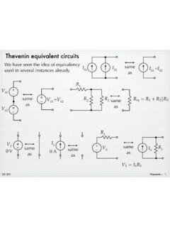
Thevenin equivalent circuits - Iowa State University
tuttle.merc.iastate.eduJun 10, 2014 · The open-circuit voltage / short-circuit current approach can be used to calculate the Thevenin equivalent for a known circuit. Consider the circuit from slide 4: + – V S R 1 R 2 I S 9V 6 mA 1.5 k! 3 k! Open-circuit voltage – Use whatever method you prefer. We’ll use node voltage in this case. + – V S R 1 R 2 I S v a + – v oc YRF= YD ...

Series and parallel combinations
tuttle.merc.iastate.eduEE 201 series/parallel combinations – 12 Breaking down networks using series and parallel R 3 R 4 R 5 R eq R 2 But not all circuits are simple R 1 combinations of series or parallel resistors. The initial example circuit clearly has some things that are in series and some elements that have a parallel-type connection.
superposition - Iowa State University
tuttle.merc.iastate.eduEE 201 superposition – 2 2va + 6vb = 2V 8va 2vb = 36V Solving gives: v a = 5 V, v b = 2 V 8v a 2v b = 0 2v a + 6v b = 2V Solving gives: and 2v a + 6v b = 0 8v a 2v b = 36V A math problem: Mathematically, we can solve the simultaneous equations a piece at a
npn Bipolar Junction Transistor - Iowa State University
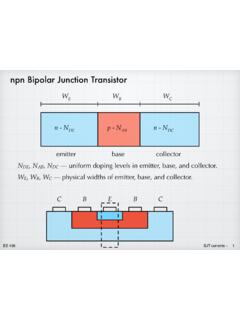
tuttle.merc.iastate.edujunction — very surprising! EE 436 BJT currents – 6 The electron current in the base is determined by the boundary ... External (terminal) currents. All currents depend on V BE in exactly the same way. Although it is a messy exponential, they …
Diffusion of dopants in silicon - Iowa State University
tuttle.merc.iastate.eduSolid-solubility limit In principle, the surface concentration that shows up in the diffusion expression could be controlled by changing the flow of a gaseous source of the dopant. (More about this later.) In practice, however, N s will be determined by the “solid solubility limit” of the dopant in the silicon. This is the thermodynamic ...
Related documents

Lecture 20 Bipolar Junction Transistors (BJT): Part 4 ...
alan.ece.gatech.edu•Warning: Just like when a diode voltage exceeds a certain value, the non-linear behavior of the diode leads to distortion of the current/voltage curves (see previous lecture), if the inputs/outputs exceed certain limits, the full Ebers -Moll model ... Applying a voltage divider: BE /v.
Thevenin equivalent circuits - Iowa State University
tuttle.merc.iastate.eduJun 10, 2014 · The open-circuit voltage / short-circuit current approach can be used to calculate the Thevenin equivalent for a known circuit. Consider the circuit from slide 4: + – V S R 1 R 2 I S 9V 6 mA 1.5 k! 3 k! Open-circuit voltage – Use whatever method you prefer. We’ll use node voltage in this case. + – V S R 1 R 2 I S v a + – v oc YRF= YD ...

Lecture 19 - MIT
web.mit.eduVoltage divider at input: Voltage divider at output: Loaded voltage gain: v in=R vs Rin +Rs vout =RL Avovin Rout +RL vout vs = Rin Rin +RS Avo RL RL +Rout +-vin +-Avovin vout Rout +-Rin Rs vs +-RL unloaded circuit output loading input loading. 6.012 Spring 2007 Lecture 19 8 Small-signal voltage gain Avo: draw small-signal

Chapter 6: Voltage Regulator - Ajlon Tech
www.ajlontech.comA feedback voltage obtained from voltage divider R 1 and R 2 is applied to the op-amp’s non-inverting input and compared to the Zener voltage to control the drive current to the transistor. The current through resistor R S is thus controlled to drop a voltage across R S so that the output voltage is maintained.

Data Sheet ADP172 - Analog Devices
www.analog.comApr 21, 2021 · Subtract the current from the external resistor divider network in the case of adjustable voltage output (as with the ADP172) from the ground current measured. 2 Based on an end-point calculation using 1 mA and 300 mA loads.

VOLTAGE TRANSFORMERS
www.gegridsolutions.comwatts at rated secondary voltage when rated phase-to-ground voltage is impressed across the capacitance voltage divider. The rated burden of the device is the sum of the watt burdens that may be impressed on both secondary windings simultaneously. Adjustment capacitors are provided in the device for connecting in parallel with the

Operational amplifier stability compensation methods for ...
www.st.comFigure 9. Voltage follower configuration Figure 10. Closed loop gain measured for a voltage follower configuration Voltage Follower Configuration - Closed Loop Gain-40-30-20-10 0 10 20 1.E+03 1.E+04 1.E+05 1.E+06 1.E+07 Frequency (Hz) Gain (dB) Gain without CL Gain with CL = 550 pF TS507 : Vcc = 5 V Vicm = 2,5 V T = 25 °C RL = 10 kΩ Without ...