
The Bandgap Reference
While simple and robust, the band-gap reference in Figure 6(a) suffers from several undesirable effects: 1) the output tends to contain sub-stantial flicker (and thermal) noise con - tribution from the op amp and M 1 and M 2, 2) the circuit potentially exhibits poor supply rejection, especially due to that of the op amp, 3) if driving a
Download The Bandgap Reference

Information
Domain:
Source:
Link to this page:
Documents from same domain
Fundamentals of Chemical Reactor Theory1 - …
www.seas.ucla.edu1 UNIVERSITY OF CALIFORNIA, LOS ANGELES Civil & Environmental Engineering Department Fundamentals of Chemical Reactor Theory Michael K. Stenstrom

Introduction to Switched-Capacitor Circuits
www.seas.ucla.eduChapter 12. Introduction to Switched-Capacitor Circuits 398 Vout Vin C1 Vout V C C1 2 AB AB in0 (a) (b) Vin VA Vin0 t0 t Vin0 C1 C2 (c) Vout Figure 12.5. Circuit of Fig. 12.4 in (a) sampling mode, (b) amplification mode.

Noise in RF Design - Engineering
www.seas.ucla.eduEE215C B. Razavi Win. 13 HO #2 17 Example Noise Figure At high frequencies, it becomes difficult to measure the input-referred noise …
CMOS technology characterization for analog and …
www.seas.ucla.eduCMOS Technology Characterization for Analog and RF Design Behzad Razavi, Member, IEEE Abstract— The design of analog and radio-frequency (RF) circuits in CMOS technology becomes increasingly more difficult as device modeling faces new challenges in deep submicrometer processes and emerging circuit applications. The …

Analog Integrated Circuit Design - Engineering
www.seas.ucla.eduEE 215A HO#1 Fall 2014 Analog Integrated Circuit Design Instructor: Behzad Razavi 56-147D, Eng. IV
International Journal of Heat and Mass Transfer - …
www.seas.ucla.eduS;T refers to heat of mixing due to temperature gradient 638 A. d’Entremont, L. Pilon/International Journal of Heat and Mass Transfer 75 (2014) 637–649 depends on the ion concentration distribution and vice versa.

Seismic Code Requirements - Engineering
www.seas.ucla.eduBuilding Response Analysis zIn general, three types of analyses are done to design buildings subjected to earthquakes – Response History Analysis zLinear or nonlinear approach to calculate time varying responses (P, M, V, δ) – Response Spectrum Analysis zLinear approach to calculate modal responses (peak values) and combine modal responses
Physics of high-pressure helium and argon radio-frequency ...
www.seas.ucla.eduThe physics of helium and argon rf discharges have been investigated in the pressure range from 50 to 760 Torr. The plasma source consists of metal electrodes that are perforated to allow the gas to
Fall 14 HO #8 - School of Engineering and Applied Science
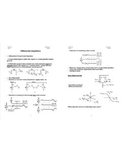
www.seas.ucla.eduEE215A B. Razavi Fall 14 HO #8 1 Differential Amplifiers Differential & Single-Ended Operation - A single-ended signal is taken with

L.Vandenberghe ECE133A(Fall2018) 5.Orthogonalmatrices
www.seas.ucla.eduProof thesquareddistanceofb toanarbitrarypointAx inrange„A”is kAx bk2 = kA„x xˆ”+ Axˆ bk2 (wherexˆ = ATb) = kA„x xˆ”k2 + kAxˆ bk2 +2„x xˆ”TAT„Axˆ b” = kA„x xˆ”k2 + kAxˆ bk2 = kx xˆk2 + kAxˆ bk2 kAxˆ bk2 withequalityonlyifx = xˆ line3followsbecauseAT„Axˆ b”= xˆ ATb = 0 line4followsfromATA = I Orthogonalmatrices 5.18
Related documents

Optical Physics of Quantum Wells - Stanford EE
ee.stanford.eduThe simplest "k.p" band theory says that the electron effective mass, me, and the light hole effective mass, mlh, are approximately equal and proportional to the band gap energy. For GaAs, which has a band gap energy of ~ 1.5 eV, the actual values are me ~ 0.069 mo and mlh ~ 0.09 mo, where mo is the free electron mass.

The Use of UV-visible Spectroscopy to Measure the Band Gap ...
mmrc.caltech.eduThe possibility of degradation from high energy Figure 1 Direct (allowed) band gap Tauc plot (solid black) and absorption coefficient (solid red) plot of MoS 2. Extrapolation of (αhν)2 to the x-intercept using the low energy exponential tail region results in an underestimate of the band gap (dashed blue and dashed orange). In this case, the

Simple Method of Measuring the Band Gap Energy Value
www.perkinelmer.comIn order for an electron to jump from a valence band to a conduction band, it requires a specific minimum amount of energy for the transition, the band gap energy.1,2 A diagram illustrating the bandgap is shown in Figure 1. Measuring the band gap is important in the semiconductor and nanomaterial industries. The band gap energy of insulators is ...

Determination of the Band-Gap of a Semiconductor ...
www.ijsr.netsilicon photonics. They calculate the energy band variation as a function of strain and inferred that the crossover from indirect to direct band gap occurs for a tensile in-plane strain of 1.9%. The effective masses of density of states are deduced from the calculated conduction and valence band density of states.

Kronig-Penney Model
yclept.ucdavis.eduCan you find any energy gap between the first and second band? – Zoom into the figure in order to determine the size of the bandgap. Note that you will obtain too large a value if you plot in large steps. Steps of 0.1 eV, e.g., are too large here. For nearly free electrons, the following can be shown (compare Kittel or Hook&Hall):

CHAPTER 4 – THE SEMICONDUCTOR IN EQUILIBRIUM
blogs.cae.tntech.eduAssume the Fermi energy is 0.25eV below the conduction band. The value of N c for Silicon at T =300KisN c =2.8x1019 cm-3. Calculate the probability that a state in the conduction band is occupied by an electron and calculate the thermal equilibrium electron concentration in silicon at T= 300 K. 2. Assume that the Fermi energy is 0.27eV above the

LABORATORY MANUAL FOR ENERGY BAND GAP EXPERIMENT
www.nitj.ac.inTheory: A semi-conductor (either doped or intrinsic) always possesses an energy gap between its valence and conduction bands (fig.1). For the conduction of electricity, a certain amount of energy is to be given to the electron so that it can jump from the valence band to the conduction band. The energy so needed is the measure of the energy gap ...