Transcription of Introduction to Switched-Capacitor Circuits
1 12 Introduction to switched -CapacitorCircuitsOur study of amplifiers in previous chapters has dealt with only cases where the input signal iscontinuously available and applied to the circuit and the output signal is continuously continuous-time Circuits , such amplifiers find wide application in audio, video, and high-speed analog systems. In many situations, however, we may sense the input only at periodic instantsof time, ignoring its value at other times. The circuit then processes each sample, producing avalid output at the end of each period. Such Circuits are called discrete-time or sampled-data this chapter , we study a common class of discrete-time systems called Switched-Capacitor (SC) Circuits .
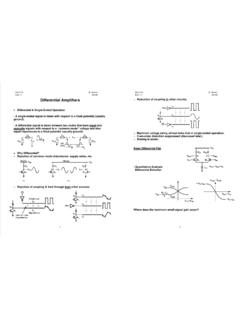
2 Our objective is to provide the foundation for more advanced topics such as filters,comparators, ADCs, and DACs. Most of our study deals with Switched-Capacitor amplifiers butthe concepts can be applied to other discrete-time Circuits as well. Beginning with a general viewof SC Circuits , we describe sampling switches and their speed and precision issues. Next, weanalyze Switched-Capacitor amplifiers, considering unity-gain, noninverting, and multiply-by-twotopologies. Finally, we examine a Switched-Capacitor General ConsiderationsIn order to understand the motivation for sampled-data Circuits , let us first consider the simplecontinuous-time amplifier shown in Fig.
3 (a). Used extensively with bipolar op amps, thiscircuit presents a difficult issue if implemented in CMOS technology. Recall that, to achieve ahigh voltage gain, the open-loop output resistance of CMOS op amps is maximized, typicallyapproaching hundreds of kilo-ohms. We therefore suspect thatR2heavily drops the open-loopgain, degrading the precision of the circuit. In fact, with the aid of the simple equivalent circuit395 chapter 12. Introduction to Switched-Capacitor Circuits396RR12outVinVRR12outVinVAVRoutX VXv (a)(b)Figure (a) Continuous-time feedback amplifier, (b) equivalent circuit of (a).
4 Shown in Fig. (b), we can write Av(Vout VinR1+R2R1+Vin) RoutVout VinR1+R2=Vout;(12:1)and henceVoutVin= R2R1 Av RoutR21+RoutR1+Av+R2R1:(12:2)Equation ( ) implies that, compared to the case whereRout=0, the closed-loop gain suffersfrom inaccuracies in both the numerator and the denominator. Also, the input resistance of theamplifier, approximately equal toR1, loads the preceding stage while introducing thermal the circuit of Fig. (a), the closed-loop gain is set by the ratio reducing the open-loop gain of the op amp, we postulate that the resistors can be replaced bycapacitors [Fig. (a)]. But, how is the bias voltage at nodeXset?
5 We may add a large feedbackoutVinV(a)CC12 XoutVinV(a)CC12 XRFF igure (a) Continuous-time feedback amplifier using capacitors , (b) use of resistor to definebias as in Fig. (b), providing dc feedback while negligibly affecting the ac behavior of theamplifier in the frequency band of interest. Such an arrangement is indeed practical if the circuitsensesonlyhigh-frequency signals. But suppose, for example, the circuit is to amplify a voltageChapter 12. Introduction to Switched-Capacitor Circuits397tinVoutVFigure Step response of the amplifier of Fig. (b).step. Illustrated in Fig. , the response contains a step change due to the initial amplificationby the circuit consisting ofC1;C2, and the op amp, followed by a tail resulting from the loss ofcharge onC2throughRF.
6 From another point of view, the circuit may not be suited to amplifywidebandsignals because it exhibits a high-pass transfer function. In fact, the transfer function isgiven byVoutVin(s) RF1C2sRF+1C2s 1C1s( )= RFC1sRFC2s+1;( )indicating thatVout=Vin C1=C2only if! (RFC2) above difficulty can be remedied by increasingRFC2, but in many applications the requiredvalues of the two components become prohibitively large. We must therefore seek other methodsof establishing the bias while utilizing capacitive feedback us now consider the Switched-Capacitor circuit depicted in Fig. , where three switchescontrol the operation:S1andS3connect the left plate ofC1toVinand ground, respectively, andoutVinVCC12S3S1S2 Figure unity-gain feedback.
7 We first assume the open-loop gain of the op amp is very largeand study the circuit in two phases. First,S1andS2are on andS3is off, yielding the equivalentChapter 12. Introduction to Switched-Capacitor Circuits398outVinVC1outVVCC12 ABABin0(a)(b)VinVAVin0tt0 Vin0C1C2(c)outVFigure Circuit of Fig. in (a) sampling mode, (b) amplification of Fig. (a). For a high-gain op amp,VB=Vout 0, and hence the voltage acrossC1isapproximately equal toVin. Next, att=t0,S1andS2turn off andS3turns on, pulling nodeAtoground. SinceVAchanges fromVin0to 0, the output voltage must change from zero toVin0C1= output voltage change can also be calculated by examining the transfer of charge.
8 Notethat the charge stored onC1just beforet0is equal , the negative feedbackthroughC2drives the op amp input differential voltage and hence the voltage acrossC1to zero(Fig. ). The charge stored onC1att=t0must then be transferred toC2, producing an outputoutVCC12in0outVCC12 Qin0Q00 Figure of charge equal toVin0C1=C2. Thus, the circuit amplifiesVin0by a factor ofC1= attributes of the circuit of Fig. distinguish it from continuous-time implementa-tions. First, the circuit devotes some time to sample the input, setting the output to zero andproviding no amplification during this period.
9 Second, after sampling, fort>t0, the circuit ignoresthe input voltageVin, amplifying the sampled voltage. Third, the circuit configuration changesChapter 12. Introduction to Switched-Capacitor Circuits399considerably from one phase to another, as seen in Fig. (a) and (b), raising concern about is the advantage of the amplifier of Fig. over that in Fig. In addition tosampling capability, we note from the waveforms depicted in Fig. that afterVoutsettles, thecurrent throughC2approaches zero. That is, the feedback capacitor does not reduce the open-loopgain of the amplifier if the output voltage is given enough time to settle.
10 In Fig. , on the otherhand,R2continuously loads the Switched-Capacitor amplifier of Fig. lends itself to implementation in CMOS technol-ogy much more easily than in other technologies. This is because discrete-time operations requireswitches to perform sampling as well as a high input impedance to sense the stored quantities withno corruption. For example, if the op amp of Fig. incorporates bipolar transistors at its input,the base current drawn from the inverting input in the amplification phase [Fig. (b)] createsan error in the output voltage. The existence of simple switches and a high input impedance havemade CMOS technology the dominant choice for sampled-data foregoing discussion leads to the conceptual view illustrated in Fig.