Transcription of 60 A VRPower Smart Power Stage (SPS) Module …
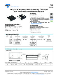
1 SiC645, Siliconix S20-0486-Rev. C, 29-Jun-20201 Document Number: 65424 For technical questions, contact: DOCUMENT IS SUBJECT TO CHANGE WITHOUT NOTICE. THE PRODUCTS DESCRIBED HEREIN AND THIS DOCUMENTARE SUBJECT TO SPECIFIC DISCLAIMERS, SET FORTH AT A VRPower Smart Power Stage (SPS) Module with IntegratedHigh Accuracy Current and Temperature MonitorsDESCRIPTIONThe SiC645 is a Smart VRPower device that integrates a high side and low side MOSFET, a high performance driver with integrated bootstrap FET. The SiC645 offers high accuracy current and temperature monitors that can be fed back to the controller and doubler to complete a multiphase DC/DC system. They simplify design and increase performance by eliminating the DCR sensing network and associated thermal compensation. Light-load efficiency is supported via a dedicated left control pin.
2 An industry leading thermally enhanced dual cooled, 5 mm x 5 mm PowerPAK MLP package allows minimal overall PCB real estate and low profile devices feature a V (SiC645A) or 5 V (SiC645) compatible tri-state PWM input that, working together with multiphase PWM controllers, will provide a robustsolution in the event of abnormal operating conditions. The SiC645 also improves system performance and reliability with integrated fault protection of UVLO, over-temperature and over-current. An open-drain fault reporting pin simplifies the handshake between the Smart VRPower device and multiphase controllers and can be used to disable the controller during start-up and fault Input range: V to 18 V Supports 60 A DC current Compatible with V (SiC645A) and 5 V (SiC645) tri-state PWM Down slope current sensing 3 % accuracy current monitor (IMON) with REFIN input 8 mV/ C temperature monitor with OT flag Dedicated low side FET control input Fault protection- High side FET short and over-current protection- Over-temperature protection- VCC and VIN under voltage lockout (UVLO) Open drain fault reporting output Up to 2 MHz switching frequency Material categorization.
3 For definitions of compliance please see High frequency and high efficiency VRM and VRD Core, graphic, and memory regulators for microprocessors High density VR for server, networking, and cloud computing POL DC/DC converters and video gaming consoles TYPICAL APPLICATION DIAGRAM Fig. 1 - Typical Application Block DiagramMultiphasecontrollerPHASEBOOT+5 VENTMONS hoot-throughprotectionSmartcontrolVCCPVC CPVCCGNDVIN+12 VGNDLOUTIMONREFINCS#nCSRTN#nPWMPWMTEMPFA ULT#LGCTRLCOUTVOUTSWVCCSiC645 GNDSiC645, Siliconix S20-0486-Rev. C, 29-Jun-20202 Document Number: 65424 For technical questions, contact: DOCUMENT IS SUBJECT TO CHANGE WITHOUT NOTICE. THE PRODUCTS DESCRIBED HEREIN AND THIS DOCUMENTARE SUBJECT TO SPECIFIC DISCLAIMERS, SET FORTH AT APPLICATION CIRCUIT WITH SiC645 Fig. 2 - Typical Application Circuit VCCVSENVCORERGNDVCOREVSAENVCORE+ VGNDADDRESSVCCSENVSACONFIGVCCSVCOREPGVCO REVSENVSARGNDVSAVCCSCSRTNVSACSVSAPWMVSAT EMPVSASiC645 PWMIMONREFINTMONLGCTRLSWVINVINVCCBOOTFAU LT#5 VPVCCGND5 VPHASECSRTN1CS1 PWM1 TEMPVCORESiC645 PWMIMONREFINTMONLGCTRLSWVINVINVCCBOOTFAU LT#5 VPVCCGND5 VPHASECSRTN2CS2 PWM2CS3-5 CSRTN3-5 PWM3-5 CSRTN6CS6 PWM6 SiC645 PWMIMONREFINTMONLGCTRLPHASEVINVINVCCBOOT FAULT#5 VPVCCGND5 VSWPMSDAnPMALERTPMSCLSVDATASVCLKnSVALERT PGVSAnVRHOTnPINALERTCFPVINSENVINN phasesSiC645 PWMIMONREFINTMONLGCTRLSWVINVINVCCBOOTFAU LT#5 VPVCCGND5 VPHASE5 V5 V5 V5 VMultiphasecontrollerSiC645, Siliconix S20-0486-Rev.
4 C, 29-Jun-20203 Document Number: 65424 For technical questions, contact: DOCUMENT IS SUBJECT TO CHANGE WITHOUT NOTICE. THE PRODUCTS DESCRIBED HEREIN AND THIS DOCUMENTARE SUBJECT TO SPECIFIC DISCLAIMERS, SET FORTH AT Fig. 3 - Typical Application CircuitVCCVSENVCORERGNDVCOREENVCORED igitalmultiphase+ VVCCSVCCSLoadCSRTN1CS1 PWM1 TEMPVCORECS2-5 CSRTN2-5 PWM2-5 CSRTN6CS6 PWM6N PhasesPhase doublerPWMPWMBCSENBCSENACSRTNAPWMACSRTNB 5 VSiC645 REFINTMONFAULT#IMONLGCTRLSWVINVINVCCBOOT PWM5 VPVCCGND5 VPHASE5 VSiC645 REFINTMONFAULT#IMONLGCTRLSWVINVINVCCBOOT PWM5 VPVCCGND5 VPHASEPWMPWMBCSENBCSENACSRTNAPWMACSRTNB5 VSiC645 REFINTMONFAULT#IMONLGCTRLSWVINVINVCCBOOT PWM5 VPVCCGND5 VPHASEISL99227 BREFINTMONFAULT#IMONLGCTRLSWVINVINVCCBOO TPWM5 VPVCCGND5 VPHASE5 VVCCSP hase doublerSiC645, Siliconix S20-0486-Rev. C, 29-Jun-20204 Document Number: 65424 For technical questions, contact: DOCUMENT IS SUBJECT TO CHANGE WITHOUT NOTICE.
5 THE PRODUCTS DESCRIBED HEREIN AND THIS DOCUMENTARE SUBJECT TO SPECIFIC DISCLAIMERS, SET FORTH AT BLOCK DIAGRAM Fig. 4 - Functional Block DiagramORDERING INFORMATIONPART NUMBERMARKING CODETEMPERATURE RANGE ( C)PWM INPUT (V)PACKAGE (RoHS-compliant)SiC645 ADR-T1-GE345D-40 to + cooled PowerPAK MLP55-32 LSiC645 ALR-T1-GE345L-10 to + cooled PowerPAK MLP55-32 LSiC645 AER-T1-GE345E-40 to + cooled PowerPAK MLP55-32 LSiC645ER-T1-GE345E-40 to +1255 Dual cooled PowerPAK MLP55-32 LBOOTVCCPVCCPVCCVIN20 KPWMSWGNDNCPHASELGCTRLFAULT# (for V) VLDOHFETLFETVCC UVLO+-PHASE-+100 mVGLOR functionVINPORV(TJ) VIN UVLO+-90 A+-OCH+-PWMHPWMLVUGHVLGHOCHVCCPORVINPORH S driverLS driverAGND-PGND level shifterTMONOT+-+-V(TJ) V(Tmax.) TJ V(TJ) = V + 8 mV x TJ VCSHGH_BLANK controlDead time and shoot-throughlogicVCC-BOOT levelshifterGL_BLANK controlCSLREFINIMONREFIN + VOCH1 s pulseHFET shortCALand levelshiftPWM logicBOOT switchcontrol (for V)SiC645, Siliconix S20-0486-Rev.
6 C, 29-Jun-20205 Document Number: 65424 For technical questions, contact: DOCUMENT IS SUBJECT TO CHANGE WITHOUT NOTICE. THE PRODUCTS DESCRIBED HEREIN AND THIS DOCUMENTARE SUBJECT TO SPECIFIC DISCLAIMERS, SET FORTH AT CONFIGURATION Fig. 5 - Pinout ConfigurationPIN CONFIGURATIONPIN NUMBERNAMEFUNCTION1 LGCTRLL ower gate control signal input. LO = GL LO (LFET off). HI = normal operation (GL and GH strictly obey PWM). This pin should be driven with a logic signal, or externally tied high if not required; it should not be left floating2 VCC+5 V logic bias supply. Place a high quality low ESR ceramic capacitor (~1 F/X7R) in close proximity from this pin to GND3 PVCC+5 V gate drive bias supply. Place a high quality low ESR ceramic capacitor (~1 F/X7R) in close proximity from this pin to GND4, 6, 7, 8, 17, 18, 19, 20, 29, 33, 35 GNDGND pins are internally connected.
7 Pins 4 and 29 should be connected directly to the nearby GND paddles on package bottom. Fig. 15 shows GND paddles should be connected to the system GND plane with as many vias as possible to maximize thermal and electrical connect (This is a low side gate driver output (GL), optional to monitor for system debugging)9, 10, 11, 12,13, 14, 15, 16 SWSwitching junction node between HFET source and LFET drain. Connect directly to output inductor21, 22, 23, 27,34 VINI nput of Power Stage (to drain of HFET). Place at least 2 ceramic capacitors (10 F or higher, X5R or X7R) in close proximity across VIN and GND. Pin 27 should not be used for decoupling. For optimal performance, place as many vias as possible in the bottom side VIN paddle24 PHASER eturn of boot capacitor. Internally connected to SW node so no external routing required for SW connection25 BOOTF loating bootstrap supply pin for the upper gate drive.
8 Place a high quality low ESR ceramic capacitor ( F/X7R to F/X7R)i n close proximity across BOOT and PHASE pins26 FAULT#Open drain output pin. Any fault (over-current, over-temperature, shorted HFET, or POR / UVLO) will pull this pin to ground. This pin may be connected to the controller enable pin or used to signal a fault at the system level28 PWMPWM input of gate driver, compatible with V and 5 V tri-state PWM signal30 REFINI nput for external reference voltage for IMON signal. This voltage should be between V and V. Connect REFIN to the appropriate current sense input of the controller. Place a high quality low ESR ceramic capacitor (~ F) in close proximity from this pin to GND31 IMONC urrent monitor output, referenced to REFIN. IMON will be pulled high (to REFIN + V) to indicate an HFET shorted or over-current fault. Connect the IMON output to the appropriate current sense input of the controller.
9 No more than 56 pF capacitance can be directly connected across IMON and REFIN pins. With a 100 series resistor, up to 470 pF may be used32 TMONT emperature monitor output. For multiphase, the TMON pins can be connected together as a common bus; the highest voltage (representing the highest temperature) will be sent to the PWM controller. TMON will be pulled high (to V) to indicate an over-temperature fault. No more than 250 pF total capacitance can be directly connected across TMON and GND pins; with a series resistor, a higher capacitance load is allowed, such as 1 k for 100 nF load142358671718192021222332313029282726 2524910111213141516 LGCTRLVCCPVCCGNDGLGNDGNDGNDGNDGNDGNDGNDV INVINVINSWSWSWSWSWSWSWSWIMONREFINGNDPWMV INFAULT#BOOTPHASETMONVINGNDGND 333435 SiC645, Siliconix S20-0486-Rev. C, 29-Jun-20206 Document Number: 65424 For technical questions, contact: DOCUMENT IS SUBJECT TO CHANGE WITHOUT NOTICE.
10 THE PRODUCTS DESCRIBED HEREIN AND THIS DOCUMENTARE SUBJECT TO SPECIFIC DISCLAIMERS, SET FORTH AT Stresses beyond those listed under Absolute Maximum Ratings may cause permanent damage to the device. These are stress ratings only, and functional operation of the device at these or any other conditions beyond those indicated in the operational sections of the specifications is not implied. Exposure to absolute maximum rating conditions for extended periods may affect device reliabilityNotes(1) JA is measured in free air with the component mounted on a high effective thermal conductivity test board with direct attach features(2)For JC, the case temperature location is the center of the exposed metal pad on the package underside(3)These ratings vary with PCB layout and operating condition, and limited by device temperature and thermal shutdown trip pointABSOLUTE MAXIMUM RATINGSELECTRICAL PARAMETER SYMBOLCONDITIONSLIMITUNIT Supply voltageVCC, PVCC to +6 VInput supply voltageVIN to +25 PHASE, SW voltage VPH-GND, VSW-GNDGND - 10 V, < 20 ns pulse width, 10 to +25 BOOT voltageVBOOT_GND to +36 Other I/O pin voltage to VCC + junction temperature (plastic package)150 CMaximum storage temperature range-65 to +150 Lead (Pb)