Class e f amplifiers
Found 8 free book(s)
EDCh 2 other linear circuits - Analog Devices
www.analog.comsection 2.13: programmable gain amplifiers 2.87 section 2.14: audio amplifiers 2.95 amplifiers 2.95 vcas (voltage controlled amplifiers) 2.98 line drivers and receivers 2.101 audio line receivers 2.101 audio line drivers 2.103 class-d power amplifiers 2.105 section 2.15: auto-zero amplifiers 2.119 chopper amplifiers 2.119
RF Power Amplifiers - QSL.net
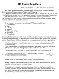
www.qsl.net• The same as in Class-A, the DC bias applied to the transistor determines the Class-B operation. • Class-B amplifiers are more efficient than Class-A amplifiers. The instantaneous efficiency of a Class-B Power Amplifier varies with the output voltage and for an ideal PA reaches π/4 (78.5 %) at PEP. However, they are much less linear.
An introduction to LLC resonant half-bridge converter
www.st.com2.3.1 Operation at resonance (f = fR1) ... Borrowing the terminology from power amplifiers, Resonant tank circuit Switch network Vin dc Vout ac Resonant Inverter Resonant tank circuit Switch network Vin ... called "class D resonant inverters". As to resonant tanks, with two reactive element s (one L and one C) there are a total of eight ...

RF and Microwave Power Amplifier Design
nfs.gongkong.comInverse Class F 264 Class E with Shunt Capacitance 271 Class E with Parallel Circuit 279 Class E with Transmission Lines 286 Broadband Class E Circuit Design 299 Practical High Efficiency RF and Microwave Power Amplifiers 305 Chapter 8. Broadband Power Amplifiers 315 Bode-Fano Criterion 316
Class E/F Amplifiers - University of California, Berkeley
rfic.eecs.berkeley.eduIn class-F amplifiers, the waveforms are assumed to be composed entirely of low-order harmonic components with simple constraints (such as being maximally flat at a certain point, etc.). The solution for switching amplifiers is less obvious because the constraint imposed by

Cascaded Amplifiers -- Two-Stage Op Amp Design
class.ece.iastate.edustage amplifiers are actually three-stage amplifiers. These invariable have a very small gain on the ... e de de de e t e r l t le Input e t 2. Two-stage Architectural Choices Which of these 2304 choices can be used to build a good op amp? All of them !! ted d s n- …
Lecture 17: Clock Recovery - Stanford University
web.stanford.edu• Other: Signal amplifiers, Supply de-coupling. MAH EE 371 Lecture 17 19 Variable delay elements • Delays in CMOS are usually generated by RC elements. e.g.: • Delay can be controlled by varying R (or I), C, or Vinv. • All of the above can …

Obsolete Product(s) - STMicroelectronics
www.st.comGv Open loop voltage gain f = 1 kHz 80 dB Gv Closed loop voltage gain f = 1 kHz 25.5 26 26.5 dB d Total harmonic distortion Po = 0.1 to 14 W; RL= 4 Ω f = 40 to 15 000 Hz; f = 1 kHz Po = 0.1 to 9 W, f = 40 to 15 000Hz RL= 8 Ω 0.08 0.03 0.5 % d2 Second order CCIF intermodulation distortion PO = 4W, f2 – f1 = 1kHz, RL = 4Ω 0.03 % d3 Third ...