Fet Input Amplifier
Found 7 free book(s)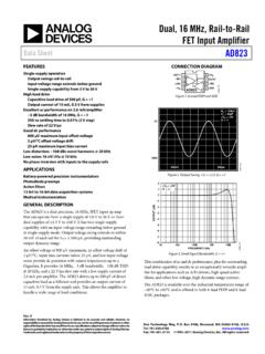
Dual, 16 MHz, Rail-to-Rail FET Input Amplifier Data Sheet ...
www.analog.comFET Input Amplifier Data Sheet AD823 Rev. E Information furnished by Analog Devices is believed to be accurate and reliable. However, no responsibility is assumed by Analog Devices for its use, nor for any infringements of patents or other rights of third parties that may result from its use. Specifications subject to change without notice. No

TL082 Wide Bandwidth Dual JFET Input Operational …
www.ti.comTL082 Wide Bandwidth Dual JFET Input Operational Amplifier Check for Samples: TL082-N 1FEATURES DESCRIPTION These devices are low cost, high speed, dual JFET 23• Internally Trimmed Offset Voltage: 15 mV input operational amplifiers with an internally trimmed • Low Input Bias Current: 50 pA input offset voltage ( BI-FET II™ technology). They

OPA657 1.6-GHz, Low-Noise, FET-Input Operational …
www.ti.comOPA657 ±5 1600 700 4.8 Gain of +7 stable FET Input OPA656 ±5 230 290 7 Unity-Gain Stable FET-Input OPA659 ±6 350 2550 8.9 Unity-Gain Stable FET-Input LMH6629 5 4000 1600 0.69 Gain of +10 stable Bipolar Input THS4631 ±15 210 1000 7 Unity-Gain Stable FET-Input Programmable Gain (5 kΩ/ 20 kΩ) OPA857 5 4750 220 — Transimpedance Amplifier

SA612A Double-balanced mixer and oscillator - NXP
www.nxp.comThe Gilbert cell is a differential amplifier (IN_A and IN_B pins) that drives a balanced switching cell. The differential input stage provides gain and ... equivalent AC input impeda nce is approximately 1.5 k 3 pF through 50 MHz. IN_A and ... The FET offers good isolation, simplicity, and low current, while the bipolar transistors provide the ...

7. Low-Noise Amplifier Design - Cambridge University Press
www.cambridge.orgMinimize the noise of the amplifier for a given signal source impedance to approach transistor minimum noise figure/factor NF MIN /F MIN Input and output matching to source and load. Maximize gain (G) and linearity (IIP3) Reduce DC power P DC => conflict with F and IIP3 F=FMIN Rn Gs ∣Ys−Ysopt∣ 2 FoMLNA= G× IIP3× f F−1 PDC
EDCh 2 other linear circuits - Analog Devices
www.analog.com(A) HOS-100 Bipolar, (B) LH0033 FET Input If high input impedance is required, a dual FET can be used as an input stage ahead of a complementary emitter follower, as shown in Figure 2.1B. This form of the buffer circuit was implemented by both National Semiconductor Corporation as the LH0033, and by Analog Devices as the ADLH0033.

High Performance Regenerative Receiver
www.arrl.orgvery effective input attenuator that serves as an RF GAIN control. As be- fore, the RF stage is inductively coupled to the detector via Ll. This maximizes signal transfer to the de- tector without loading it down. JFET Q2 operates as a tickler feedback or Armstrong regenerative detector cir- cuit. This receiver uses a 2N4416