Mosfet Output
Found 7 free book(s)
Lecture 10 MOSFET (II)
ocw.mit.eduOct 13, 2005 · 3µm nchannel MOSFET Output characteristics (VGSGS =0.5 V ): 6.012 Microelectronic Devices and Circuits Fall 2005 Lecture 1011 Transfer characteristics in saturation (DSV=3 V ): ++ 6.012 Microelectronic Devices and Circuits Fall 2005 Lecture 1012
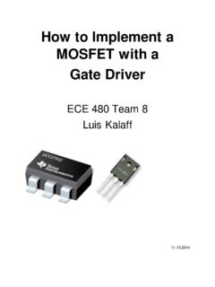
How to Implement a MOSFET with a Gate Driver
www.egr.msu.eduNov 13, 2014 · A MOSFET driver IC translates TTL or CMOS logical signals, to a higher voltage and higher current, with the goal of rapidly and completely switching the gate of a MOSFET. An output pin of a microcontroller is usually adequate to drive a small-signal logic level MOSFET. However driving larger MOSFETs is a different story. Large MOSFETs have
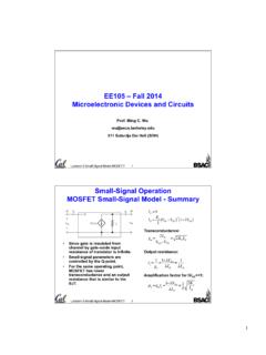
EE105 – Fall 2014 Microelectronic Devices and Circuits
inst.eecs.berkeley.eduLecture13-Small Signal Model-MOSFET 11 C-E and C-S Amplifiers Output Resistance Lecture13-Small Signal Model-MOSFET 12 C-E and C-S Amplifiers Output Resistance (cont.) For comparable bias points, output resistances of C-S and C-E amplifiers are similar. Apply test source v x and find i x (with v i = 0) v be =0 → g m v be =0 ∴R out = v x i x ...

MC34152 - MOSFET Driver, High Speed, Dual
www.onsemi.comMOSFET Driver, High Speed, Dual The MC34152/MC33152 are dual noninverting high speed drivers specifically designed for applications that require low current digital signals to drive large capacitive loads with high slew rates. These ... • Output Rise and Fall Times of …

MOSFET AMPLIFIER - Learn LTSpice: A Tutorial
learn-ltspice.weebly.comAC signal to the amplifier and coupling a load at the output. For this we need two capacitors, one coupling signal to the Gate of the MOSFET, and the other at the Drain coupling the load as shown in the circuit. Let us first consider that the input signal is of low frequency like audio frequency (20 Hz –20 kHz); for this range the MOSFET Gate
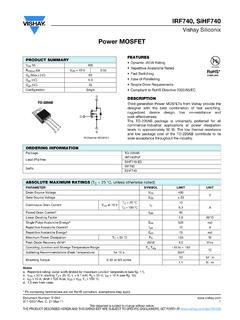
Power MOSFET - Vishay Intertechnology
www.vishay.comN-Channel MOSFET G D S TO-220AB G D S Available Available ORDERING INFORMATION Package TO-220AB Lead (Pb)-free IRF740PbF Lead (Pb)-free and halogen-free IRF740PbF-BE3 ABSOLUTE MAXIMUM RATINGS (TC = 25 °C, unless otherwise noted) PARAMETER SYMBOL LIMIT UNIT Drain-source voltage VDS 400 V Gate-source voltage VGS ± 20 Continuous drain …
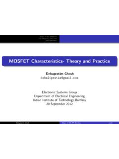
MOSFET Characteristics- Theory and Practice
www.ee.iitb.ac.inBasics of the MOSFET The MOSFET Operation The Experiment The MOS Transistor Operating Regions of the MOSFET TheMOSTransistor Once the threshold has been crossed, we need to make the electrons move, i.e. set up a current. For this, we need two more terminals- Source (S) and Drain (D), and a potential across them to control the flow of electrons.