Vlsi Layout
Found 7 free book(s)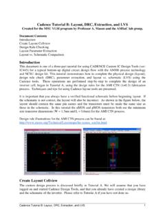
Cadence Tutorial B: Layout, DRC, Extraction, and LVS
www.egr.msu.eduCadence Tutorial B: Layout, DRC, Extraction, and LVS Created for the MSU VLSI program by Professor A. Mason and the AMSaC lab group. Document Contents Introduction Create Layout Cellview Design Rule Checking Layout Parameter Extraction Layout vs. …

Introduction to CMOS VLSI Design - University of Notre Dame
www3.nd.edu2 Design Rules CMOS VLSI Design Slide 3 Layout Overview Minimum dimensions of mask features determine: – transistor size and die size – hence speed, cost, and power “Historical” Feature size f = gate length (in nm) – Set by minimum width of polysilicon – Other minimum feature sizes tend to be 30 to 50% bigger. Design or Layout Rules: rules ...
Introduction to Analog Layout Design - SMDP-C2SD
smdpc2sd.gov.inAnalog VLSI Design. 23 January 2016 3 Analog Design Flow • Electrical Design • Physical Design • Fabrication and Testing • Final Product. 23 January 2016 4 ... MOS transistor Layout • Parasitic resistance at source and drain must be kept as low as possible
VLSI Fabrication Process
asctbhopal.comVLSI stands for "Very Large Scale Integration". This is the field which involves packing more and more logic devices into smaller and smaller areas. Thanks to VLSI, circuits that would have ... a layout editor Silicon Foundry:Masks generation from the layer patterns in the design data base Printing: transfer the mask pattern to the
Cadence Virtuoso Tutorial - USC Viterbi
ee.usc.eduIf you need to rename those files to .cshrc or vlsi_tools.csh, use command “mv”, for example, to rename cshrc to .cshrc, you can say: mv cshrc .cshrc Convert the encoding of those two files by dos2unix command: dos2unix .cshrc dos2unix vlsi_tools.csh Create a folder named cds: mkdir cds Copy useful files to your cds directory:
Physical Design via Place-and-Route: RTL to GDS
inst.eecs.berkeley.educreate a physical layout by placing standard cells on the chip and creating wires to route between the different cells. Performs standard cell placement and routing while respecting the floorplanning/physical design constraints and routing to macros (e.g. analog macros, SRAMs). The final result is a GDS file which can be sent to the fab.
ECE 128 Synopsys Tutorial: Using the Design Compiler ...
s2.smu.edu'wire model' to make the wires take on realistic RLC characteristics as they would in an extracted layout. Or another example would be to apply a 'fanout' or 'fanin' to the inputs and outputs of your design as to simulate a realistic level of input or output driving. 1. The first step is to “LINK” your design, click File → Link Design