Search results with tag "Transimpedance"

NEP – Noise Equivalent Power - Thorlabs
www.thorlabs.comThen, this output noise voltage Uout,NI [V] is divided by the transimpedance gain G [V/A], which results in the integrated input noise current Iin,NI [A]: + Ü á, L 7 K Q, W ) . (5) Please note that the transimpedance gain can be specified either for …

OPA657 1.6-GHz, Low-Noise, FET-Input Operational Amplifier ...
www.ti.comFrequency Response of 200-kΩTransimpedance Amplifier Wideband Photodiode Transimpedance Amplifier 1 An IMPORTANT NOTICE at the end of this data sheet addresses availability, warranty, changes, use in safety-critical applications, intellectual property matters and other important disclaimers. PRODUCTION DATA.
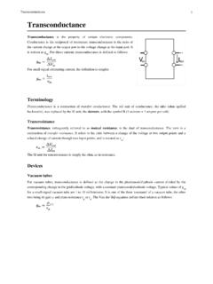
Transconductance - University of Arizona
atlas.physics.arizona.eduThe transresistance amplifier is often referred to as a transimpedance amplifier, especially by semiconductor manufacturers. The term for a transresistance amplifier in network analysis is current controlled voltage source (CCVS) . A basic inverting transresistance amplifier can be built from an operational amplifier and a single resistor. Simply
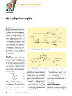
The Transimpedance Amplifier - University of California ...
www.seas.ucla.eduvoltage converter. We define the tran-simpedance gain as R I V T in = out (1) 0 I IR A in = - in (2). A A R 1 F 0 =- 0 + (3) If A 0 & 1, we have RR TF.- . Of course, a single grounded resis-tor can perform the same function [Figure 2(b)] and provide the same tran-simpedance gain. However, the principal difference is that I in sees a low impedance

Analog Engineer s Circuit Cookbook: Op Amps
www.mouser.comprovides operational amplifier (op amp) sub-circuit ideas that can be ... • ADC and amplifier design tools, noise and stability analysis, PCB and sensor tools Analog Wire Blog ... Transimpedance Amplifier Circuit.....37 Single-Supply, Low-Side, Unidirectional Current Sensing Solution ...

Designing Photodiode Amplifier Circuits with OPA128
www.ti.comthan a low resistance in a T network. See Figure 5. Although transimpedance gain (eOUT/iSIGNAL) is equivalent, the T net-work will sacrifice performance. The low feedback resis-tance will generate higher current noise (iN) and the voltage divider formed by R1/R2 multiply input offset voltage, drift, and amplifier voltage noise by the ratio of 1 ...

Design for a Wideband, Differential Transimpedance DAC ...
www.ti.com3.3V AV DD 3.3V AV DD 25 W 25 W V 1OUT V 2OUT Optional, for single-ended output referred to AV DD DAC5675A IOUT1 IOUT2 DAC IR 2 IR 2 IS IS Complementary Current Outputs Typical DAC Output Circuits www.ti.com 2 SBAA150A–April 2008–Revised October 2016
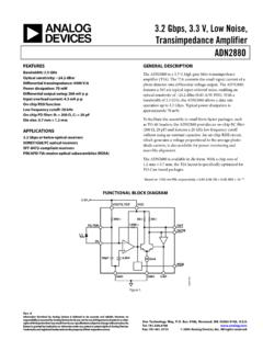
ADN2880 3.2 Gbps, 3.3 V Low Noise, …
www.analog.com3.2 Gbps, 3.3 V, Low Noise, Transimpedance Amplifier ADN2880 Rev. 0 Information furnished by Analog Devices is believed to be accurate and reliable.
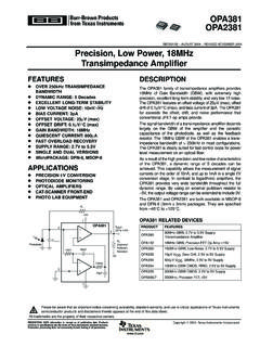
OPA381 OPA2381 Precision, Low Power, 18MHz …
www.ti.comfeatures over 250khz transimpedance bandwidth dynamic range: 5 decades excellent long-term stability low voltage noise: 10nv/√hz bias current: 3pa
Transimpedance Considerations for High-Speed …
www.ti.comGBP = 2 F R Cp · ·- 3dB F S 2 300 250 200 150 100 50 0 Maximum Achievable requency Response (MHz) 1 2 5 10 20 50 100 200 500 1000 Maximum Transimpedance Gain (k ) W