Search results with tag "Interposer"

PROGRESS AND APPLICATION OF THROUGH GLASS VIA …
www.corning.cominterposer application. Figure 2a schematically shows Si chips mounted on a Si interposer, which is then mounted on an organic substrate. The CTE mismatch causes failures when the substrates go through temperature cycles. However, if instead of a Si interposer, a glass interposer with CTE in between glass and organic is used, this warp

Recent Advances and Outlook for Heterogeneous Integration
ewh.ieee.org3D SiP with Organic Interposer for ASIC and Memory Integration (2.3D IC Integration) Li Li, Pierre Chia, Paul Ton, Mohan Nagar, Sada Patil, Jie Xue Cisco Systems, Inc. San Jose, CA 95134, U.S.A., e-mail: lili2@cisco.com. HBM_Functional µbump-pillar HBM_Mechanical Organic Interposer C4 Bumps ASIC/FPGA Organic Interposer Build-up Substrate
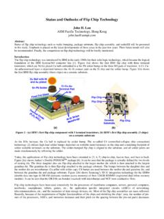
Status and Outlooks of Flip Chip Technology
www.circuitinsight.comthe organic build-up substrate, through-silicon via (TSV)-interposer, TSV-less interposer, coreless substrate, bump-on-lead (BOL), and embedded-trace-substrate (ETS) will be discussed. In order to enhance the solder joint reliability of flip chip assemblies, underfill is a must, especially for organic package substrate.

LPDDR4 200 Ball Direct Attach Interposer
www.nexustechnology.comLPDDR4 200 Ball Direct Attach Interposer www.nexustechnology.com 3 Product Configuration Table Nomenclature Data Width NEX-LP4MCI200SCDS X32

- Advanced Organic Technology for 2.5D Interposer
www.ectc.netIEEE 64th ECTC – Orlando, FL, USA Mitsuya Ishida May 27 – 30, 2014 2 • Benefits of 2.5D APX Interposer • Technology Feature of APX • Cross Section • Design Rule Comparison • Material Property • Design Rule for Impedance Control

2.1D Organic Package Technology to Realize Die-to-Die ...
www.fujitsu.comthe 2.5D structure, a 2.1D structure that integrates interposer functionality in an organic substrate has been proposed. This paper describes the 2.1D organic package that is being developed by SHINKO ELECTRIC INDUSTRIES CO., LTD. This 2.1D package can be created just by adding the functions of an organic substrate to a 2.5D
裸片到裸片接口IP的新疆域:芯片成功的需知
site.eet-china.comy Organic Substrate Data Rate: 112Gbps Line Space: >10mm Integrated Fanout (InFO) Post Fab RDL (Fanout) Data Rate: 56Gbps Line Space: >2mm, 2500 Pin Count Silicon Interposer Data Rate: 3.2 →6.4Gbps Line Space: >0.4mm, 4000 Pin Count Die/Package Size, Density & IO Count Data Rates Y Y
硅通孔(TSV)
c44f5d406df450f4a66b-1b94a87d576253d9446df0a9ca62e142.ssl.cf2.rackcdn.comf Interposer 晶圆背面所需的铜重布线层 ... Organic substrate Memory Memory Memory Die 0 Substrate Die 1 Die 2 Die 3 Die 4 Die 5 Die 6 Die 7 Die 0 Substrate Die 1 Die 2 Die 3 AP/Logic Substrate Wide I/O Die 0 Substrate Die 1 Die 2 Die 3. 硅通孔 (TSV) 2.5D TSV 集成 3D TSV 集成 …

Advanced Packaging Current Trends & Challenges
www.semiconductors.orgOrganic/ glass substrate etc. Standard organic substrate Flip-chip Wire-bond RDL FIWLP FOWLP 3D/2.5D FOPLP Silicon/ glass bridge Bump/ pillar TSV/ TGV Ceramic/ leadframe and others Advanced organic substrate Mold embedding Organic interposer FC WB CSP BGA Standard BGA Advanced LGA BGA LGA CSP Organic substrate Ceramic/ leadframe and …