Example: confidence
硅通孔(TSV)
f Interposer 晶圆背面所需的铜重布线层 ... Organic substrate Memory Memory Memory Die 0 Substrate Die 1 Die 2 Die 3 Die 4 Die 5 Die 6 Die 7 Die 0 Substrate Die 1 Die 2 Die 3 AP/Logic Substrate Wide I/O Die 0 Substrate Die 1 Die 2 Die 3. 硅通孔 (TSV) 2.5D TSV 集成 3D TSV 集成 …
Tags:
Information
Domain:
Source:
Link to this page:
Documents from same domain

'Core Power Delivery Network Analysis of Core and Coreless ...
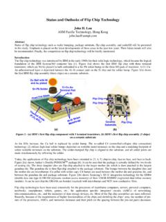
c44f5d406df450f4a66b-1b94a87d576253d9446df0a9ca62e142.ssl.cf2.rackcdn.com1 Core Power Delivery Network Analysis of Core and Coreless Substrates in a Multilayer Organic Buildup Package Ozgur Misman, Mike DeVita, Nozad Karim,
ChinalntegratedCircult CIC 中国集成电路
c44f5d406df450f4a66b-1b94a87d576253d9446df0a9ca62e142.ssl.cf2.rackcdn.comCore Power Delivery Network Analysis of Core and Coreless Substrates in a Multilayer Organic Buildup Package Ozgur Misman, Mike DeVita, Nozad Karim 渊Amkor Technology, Inc., 1900 South Price Road, Chandler, AZ85286, USA冤 ...

A New RDL-First PoP Fan-Out Wafer-Level Package Process ...
c44f5d406df450f4a66b-1b94a87d576253d9446df0a9ca62e142.ssl.cf2.rackcdn.com(C2W) bonding technology is introduced. And the results are presented of building and testing an RDL-base wafer-level Interposer PoP with a size of 12.5 x 12.5 mm2 and thickness of 0.357 mm including solder ball. The bottom side has a 3-layer RDL structure andthe top RDL for the package stacking has a 1-layer structure.

Figure 1: SOURCE: Amkor Technology, Inc.
c44f5d406df450f4a66b-1b94a87d576253d9446df0a9ca62e142.ssl.cf2.rackcdn.comsemiconductor assembly and test suppliers (OSATS) is a natural ... increasing the semiconductor content in automobiles at an exponential rate. ... IWLPC is at the forefront of packaging technology evolution. Addressing Wafer-Level Packaging, 3D Packaging, and Advanced Manufacturing & Test ...

Corporate Overview
c44f5d406df450f4a66b-1b94a87d576253d9446df0a9ca62e142.ssl.cf2.rackcdn.commade semiconductor packaging a vital contributor to system . ... outsourced semiconductor advanced packaging design, assembly and test services, Amkor helps make innovative technologies a reality. AMKOR PHILOSOPHY. We build our business by helping our . customers build theirs. OUR PRODUCT PORTFOLIO ... and packaging technology…

Data Sheet WAFR LVL PACAGING
c44f5d406df450f4a66b-1b94a87d576253d9446df0a9ca62e142.ssl.cf2.rackcdn.comData Sheet WAFR LVL PACAGING Questions? Contact us: sales@amkor.com ... With respect to the information in this document Amkor makes no guarantee or warranty of its accuracy or that the use of such information will not infringe upon the intellectual rights of third parties. Amkor shall not ... Package Level: • Preconditioning at Level 1 85°C ...

倒装芯片 BGA (FCBGA)
c44f5d406df450f4a66b-1b94a87d576253d9446df0a9ca62e142.ssl.cf2.rackcdn.com倒装芯片互连采用阵列互连的方式将晶粒贴装到基板上,以代替传统焊线。这使全 部的晶粒表面可被用于以电气方式连接到基板,与外围互连技术相比大幅度增加了

TECHNOLOGY SOLUTIONS Flip Chip Packaging
c44f5d406df450f4a66b-1b94a87d576253d9446df0a9ca62e142.ssl.cf2.rackcdn.comThe package carrier, either substrate or leadframe, then provides the connection from the die to the exterior of the package. In “standard” packaging, the interconnection between the die and the carrier is made using wire. The die is attached to the carrier face up, then a wire is bonded first to the die, then looped and bonded to the carrier.

倒装芯片 CSP (fcCSP)
c44f5d406df450f4a66b-1b94a87d576253d9446df0a9ca62e142.ssl.cf2.rackcdn.com(POSSUM™) 则使封装内天线 (AiP) 成为可能。最后,借助于铜柱凸块晶片,用来说,fcCSP 封装是非常具有吸 fcCSP 技术能够利用小节距基板布线和凸块节距的优势,在减少层数与成本的同 时优化其电气性能。(包括 5G)、适用于汽车的信息娱乐和 特色

倒装芯片封装
c44f5d406df450f4a66b-1b94a87d576253d9446df0a9ca62e142.ssl.cf2.rackcdn.com最近的封装解决方案已经开始使用另外一种被称为 tcncp(非导电浆热压)的倒装芯片互连技术。有别于焊 接和底部填充两步骤制程,tcncp 可以做到一步到位。
Related documents

Recent Advances and Outlook for Heterogeneous Integration
ewh.ieee.org3D SiP with Organic Interposer for ASIC and Memory Integration (2.3D IC Integration) Li Li, Pierre Chia, Paul Ton, Mohan Nagar, Sada Patil, Jie Xue Cisco Systems, Inc. San Jose, CA 95134, U.S.A., e-mail: lili2@cisco.com. HBM_Functional µbump-pillar HBM_Mechanical Organic Interposer C4 Bumps ASIC/FPGA Organic Interposer Build-up Substrate

Advanced Packaging Current Trends & Challenges
www.semiconductors.orgOrganic/ glass substrate etc. Standard organic substrate Flip-chip Wire-bond RDL FIWLP FOWLP 3D/2.5D FOPLP Silicon/ glass bridge Bump/ pillar TSV/ TGV Ceramic/ leadframe and others Advanced organic substrate Mold embedding Organic interposer FC WB CSP BGA Standard BGA Advanced LGA BGA LGA CSP Organic substrate Ceramic/ leadframe and …

PROGRESS AND APPLICATION OF THROUGH GLASS VIA …
www.corning.cominterposer application. Figure 2a schematically shows Si chips mounted on a Si interposer, which is then mounted on an organic substrate. The CTE mismatch causes failures when the substrates go through temperature cycles. However, if instead of a Si interposer, a glass interposer with CTE in between glass and organic is used, this warp

2.1D Organic Package Technology to Realize Die-to-Die ...
www.fujitsu.comthe 2.5D structure, a 2.1D structure that integrates interposer functionality in an organic substrate has been proposed. This paper describes the 2.1D organic package that is being developed by SHINKO ELECTRIC INDUSTRIES CO., LTD. This 2.1D package can be created just by adding the functions of an organic substrate to a 2.5D
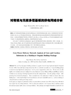
Status and Outlooks of Flip Chip Technology
www.circuitinsight.comthe organic build-up substrate, through-silicon via (TSV)-interposer, TSV-less interposer, coreless substrate, bump-on-lead (BOL), and embedded-trace-substrate (ETS) will be discussed. In order to enhance the solder joint reliability of flip chip assemblies, underfill is a must, especially for organic package substrate.
裸片到裸片接口IP的新疆域:芯片成功的需知
site.eet-china.comy Organic Substrate Data Rate: 112Gbps Line Space: >10mm Integrated Fanout (InFO) Post Fab RDL (Fanout) Data Rate: 56Gbps Line Space: >2mm, 2500 Pin Count Silicon Interposer Data Rate: 3.2 →6.4Gbps Line Space: >0.4mm, 4000 Pin Count Die/Package Size, Density & IO Count Data Rates Y Y