Search results with tag "Flip chip"

TECHNOLOGY SOLUTIONS Flip Chip Packaging
c44f5d406df450f4a66b-1b94a87d576253d9446df0a9ca62e142.ssl.cf2.rackcdn.comFlip chip solution for CSP package technology Flip Chip System in Package (SiP) Flip chip SiP package is an extension of the SiP product offering from Amkor with the device interconnect technology being flip chip rather than traditional wirebond interconnects. The package may contain multiple passive components, silicon and/or GaAs

7 Series FPGAs Data Sheet: Overview (DS180)
www.xilinx.comBare-Die Flip-Chip Bare-Die Flip-Chip and High-Performance Flip-Chip Highest Performance Flip-Chip Notes: 1. Additional memory available in the form of distributed RAM. 2. Peak DSP performance numbers are bas ed on symmetrical filter implementation. 3. Peak MicroBlaze CPU performance num bers based on microcontroller preset.
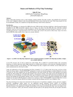
Status and Outlooks of Flip Chip Technology
www.circuitinsight.comThe flip chip technology was introduced by IBM in the early 1960s for their solid logic technology, which became the logical foundation of the IBM System/360 computer line [1]. Figure 1(a) shows the first IBM flip chip with three terminal transistors, which are Ni/Au plated Cu balls embedded in a Sn–Pb solder bump on the three I/O pads of ...
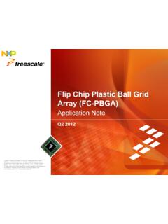
FC-PBGA, Flip Chip Plastic Ball Grid Array (FC-PBGA)
www.nxp.com•Freescale Flip-Chip PBGA body sizes range from 17x17mm to 45x45mm •BGA sphere pitch currently ranges from 0.8 to 1.27 mm Freescale Flip-Chip PBGA Package Attributes Body Size (mm) Package I/O Count Sphere Pitch (mm) Sphere Array Pkg SM Diam* (mm) 17x17 332 0.8 19x19 0.4 20x20 431 0.8 23x23 0.4 21x21 520 0.8 25x25 0.5 21x21 624 0.8 25x25 0.525
FOR IMMEDIATE RELEASE Press Release
www.semiconductorpackagingnews.comThis material can be used as an underfill for flip chip, chip scale package, ball grid array devices, package on package, and land grid array applications. It is also suitable for bare chip protection in a variety of advanced packages such as memory cards, chip carriers, hybrid circuits and multi-chip modules.

and Application of Underfill Material for Flip Chip …
www.ipc.orgIPC J-STD-030 Guideline for Selection and Application of Underfill Material for Flip Chip and Other Micropackages Developed by the Underfill Adhesives for Flip Chip Applications Task

Accelerated Thermal Cycling and Failure Mechanisms For …
nepp.nasa.govStandard Implementation of Flip Chip and Chip Scale Technology), assembly reliability projections were based on flip chip die being attached to the board. DNPs were used for calculation of the first failure and projection of failure with size of package. This is not valid for most CSPs, except possibly for a few wafer level CSPs without

Frequency Response of Thin Film Chip Resistors
www.vishay.com0402 flip chip, and (c) 0402 flip chip with L-cut trim. By extending the range of the model results indicates the presence and approximate location of the peak observed with some of the tested devices. The external modeling coefficients, figure 7, show similar results to the case size impedance performance, figure 8.

High Frequency (Up to 40 GHz) Resistor, Thin Film Surface ...
www.vishay.comThin Film Surface Mount Chip LINKS TO ADDITIONAL RESOURCES FC series chip resistors are designed with low internal reactance. They function as almost pure resistors on a very ... 0603 Flip chip 1.8 1.6 1.4 0.8 0.6 0.4 0.2 0.0 0.1 1 10 0.1 1 10 Frequency (GHz) 0.1 1 10 C = 0.0262 pF L = 0.00189 nH C = 0.0403 pF L = 0.0267 nH C = 0.0392 pF L = 0 ...

Ball Grid Array (BGA) Packaging - Intel
www.intel.comThe H-PBGA family includes Intel’s latest packaging technology - the Flip Chip (FC)-style, H-PB-GA. The FC-style, H-PBGA component uses a Controlled Collapse Chip Connect die packaged in an Organic Land Grid Array (OLGA) substrate. In addition to the typical advantages of …

Micro Structure Observation and Reliability …
www.jiep.or.jp75 Orii et al.: Micro Structure Observation and Reliability Behavior (3/14) chip die and SMT component joints are formed in a single reflow step. After a flip chip …

Fine Pitch Substrate for Cost Effective Dr. Kay Essig Flip ...
www.imapsfrance.orgFine Pitch Substrate for Cost Effective Flip Chip Package using Embedded Trace Substrate Technology Dr. Kay Essig ASE Europe May 21, 2014

JEDEC STANDARD - HALT & HASS
www.halthass.co.nzThese include flip chip, ball grid array and stacked packages with solder interconnections. Cycle frequency and soak time is more significant for solder interconnections. 4.1.3 Tin whisker cycle rate Tin whisker cycle rate shall be about 3 cycles per hour as stated in JESD22A121.

Advanced Packaging Enablement - SEMICON West
www.semiconwest.orgSpecial Requirements for SiP/FO Assembly Equipment as (Compared to a Typical Flip Chip Bonder) 1. Ability to handle face up and face down placement on same machine.

Flip Chip BGA - Signetics
www.signetics.comSignetics (HQ) 483-3 Buphung-ri Thanhyun -myun, Paju-si Gyungki-do, Republic of Korea 413-840 Tel : (Korean) 82 -31-940-7681, (English) 82-31-940-7660 Fax : 82-31-940-7888
Similar queries
Flip Chip, Flip-Chip, Flip, Chip, Ball grid array, Grid array, And Application of Underfill Material for Flip Chip, Accelerated Thermal Cycling and Failure Mechanisms For, Flip Chip and Chip, Technology, Size, Package, Frequency Response of Thin Film Chip Resistors, Intel, Micro Structure Observation and Reliability, Micro Structure Observation and Reliability Behavior, Flip chip, ball grid array, Advanced Packaging Enablement