Transcription of LM108/LM208/LM308 Operational Amplifiers - …
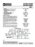
1 LM108/LM208/LM308 Operational Amplifiers December 1994. LM108/LM208/LM308 Operational Amplifiers General Description The LM108 series are precision Operational Amplifiers hav- introducing less error than devices like the 709 with 10 kX. ing specifications a factor of ten better than FET Amplifiers sources. Integrators with drifts less than 500 mV/sec and over a b55 C to a 125 C temperature range. analog time delays in excess of one hour can be made us- The devices operate with supply voltages from g 2V to ing capacitors no larger than 1 mF.
2 G 20V and have sufficient supply rejection to use unregulat- The LM108 is guaranteed from b55 C to a 125 C, the ed supplies. Although the circuit is interchangeable with and LM208 from b25 C to a 85 C, and the LM308 from 0 C to uses the same compensation as the LM101A, an alternate a 70 C. compensation scheme can be used to make it particularly insensitive to power supply noise and to make supply by- Features pass capacitors unnecessary. Y Maximum input bias current of nA over temperature The low current error of the LM108 series makes possible Y Offset current less than 400 pA over temperature many designs that are not practical with conventional ampli- Y Supply current of only 300 mA, even in saturation fiers.
3 In fact, it operates from 10 MX source resistances, Y Guaranteed drift characteristics Compensation Circuits Standard Compensation Circuit Alternate* Frequency Compensation R1 CO. Cf t R1 a R2. CO e 30 pF. TL/H/7758 1 TL/H/7758 2. **Bandwidth and slew rate are proportional to 1/Cf *Improves rejection of power supply noise by a factor of ten. **Bandwidth and slew rate are proportional to 1/Cs Feedforward Compensation TL/H/7758 3. C1995 national Semiconductor Corporation TL/H/7758 RRD-B30M115/Printed in U.
4 S. A. Absolute Maximum Ratings If Military/Aerospace specified devices are required, please contact the national Semiconductor Sales Office/. Distributors for availability and specifications. (Note 5). LM108/LM208 LM308. Supply Voltage g 20V g 18V. Power Dissipation (Note 1) 500 mW 500 mW. Differential Input Current (Note 2) g 10 mA g 10 mA. Input Voltage (Note 3) g 15V g 15V. Output Short-Circuit Duration Continuous Continuous Operating Temperature Range (LM108) b 55 C to a 125 C 0 C to a 70 C. (LM208) b 25 C to a 85 C.
5 Storage Temperature Range b 65 C to a 150 C b 65 C to a 150 C. Lead Temperature (Soldering, 10 sec). DIP 260 C 260 C. H Package Lead Temp (Soldering 10 seconds) 300 C 300 C. Soldering Information Dual-In-Line Package Soldering (10 seconds) 260 C. Small Outline Package Vapor Phase (60 seconds) 215 C. Infrared (15 seconds) 220 C. See AN-450 Surface Mounting Methods and Their Effect on Product Reliability'' for other methods of soldering surface mount devices. ESD Tolerance (Note 6) 2000V. Electrical Characteristics (Note 4).
6 LM108/LM208 LM308. Parameter Condition Units Min Typ Max Min Typ Max Input Offset Voltage TA e 25 C mV. Input Offset Current TA e 25 C 1 nA. Input Bias Current TA e 25 C 7 nA. Input Resistance TA e 25 C 30 70 10 40 MX. Supply Current TA e 25 C mA. Large Signal Voltage TA e 25 C, VS e g 15V. 50 300 25 300 V/mV. Gain VOUT e g 10V, RL t 10 kX. Input Offset Voltage 10 mV. Average Temperature Coefficient of Input 15 30 mV/ C. Offset Voltage Input Offset Current nA. Average Temperature Coefficient of Input 10 pA/ C.
7 Offset Current Input Bias Current 10 nA. Supply Current TA e a 125 C mA. Large Signal Voltage VS e g 15V, VOUT e g 10V. 25 15 V/mV. Gain RL t 10 kX. Output Voltage Swing VS e g 15V, RL e 10 kX g 13 g 14 g 13 g 14 V. 2. Electrical Characteristics (Note 4) (Continued). LM108/LM208 LM308. Parameter Condition Units Min Typ Max Min Typ Max Input Voltage Range VS e g 15V g g 14 V. Common Mode 85 100 80 100 dB. Rejection Ratio Supply Voltage 80 96 80 96 dB. Rejection Ratio Note 1: The maximum junction temperature of the LM108 is 150 C, for the LM208, 100 C and for the LM308, 85 C.
8 For operating at elevated temperatures, devices in the H08 package must be derated based on a thermal resistance of 160 C/W, junction to ambient, or 20 C/W, junction to case. The thermal resistance of the dual-in-line package is 100 C/W, junction to ambient. Note 2: The inputs are shunted with back-to-back diodes for overvoltage protection. Therefore, excessive current will flow if a differential input voltage in excess of 1V is applied between the inputs unless some limiting resistance is used. Note 3: For supply voltages less than g 15V, the absolute maximum input voltage is equal to the supply voltage.
9 Note 4: These specifications apply for g 5V s VS s g 20V and b 55 C s TA s a 125 C, unless otherwise specified. With the LM208, however, all temperature specifications are limited to b 25 C s TA s 85 C, and for the LM308 they are limited to 0 C s TA s 70 C. Note 5: Refer to RETS108X for LM108 military specifications and RETs 108AX for LM108A military specifications. Note 6: Human body model, kX in series with 100 pF. Schematic Diagram TL/H/7758 8. 3. Typical Performance Characteristics LM108/LM208.
10 Input Currents Offset Error Drift Error Closed Loop Input Noise Voltage Power Supply Rejection Output Impedance Voltage Gain Output Swing Supply Current Open Loop Large Signal Voltage Follower Frequency Response Frequency Response Pulse Response TL/H/7758 6. 4. Typical Performance Characteristics LM308. Input Currents Offset Error Drift Error Closed Loop Input Noise Voltage Power Supply Rejection Output Impedance Voltage Gain Output Swing Supply Current Open Loop Large Signal Voltage Follower Frequency Response Frequency Response Pulse Response TL/H/7758 7.