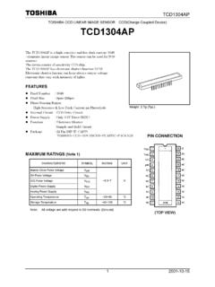
Transcription of 2048-pixel CCD Linear Sensor (B/W) for Single 5V …
1 - 1 -E05925A63 Sony reserves the right to change products and specifications without prior notice. This information does not convey any license by any implication or otherwise under any patents or other right. Application circuits shown, if any, are typical examples illustrating the operation of the devices. Sony cannot assume responsibility for any problems arising out of the use of these LimitedILX511B2048- pixel CCD Linear Sensor (B/W) for Single 5V Power Supply Bar-code ReaderDescription The ILX511B is a rectangular reduction type CCD Linear Sensor designed for bar-code POS hand scanner and optical measuring equipment built-in timing generator and clock driver ensure Single 5V power supply for easy Number of effective pixels: 2048 pixels pixel size: 14 m 200 m (14 m pitch) Single 5V power supply Ultra-high sensitivity Built-in timing generator and clock driver Built-in sample-and-hold circuit Maximum operating frequency: 2 MHzPackage 22-pin Cer-DIPA bsolute Maximum Ratings Supply voltageVDD to +7V Operating temperature 10 to +60 C Storage temperature 30 to +80 CILX511B- 2 -USE RESTRICTION NOTICE (December 1, 2003 ver.)
2 This USE RESTRICTION NOTICE ( Notice ) is for customers who are considering or currently using the CCD products ( Products ) set forth in this specifications book. Sony Corporation ( Sony ) may, at any time, modify this Notice which will be available to you in the latest specifications book for the Products. You should abide by the latest version of this Notice. If a Sony subsidiary or distributor has its own use restriction notice on the Products, such a use restriction notice will additionally apply between you and the subsidiary or distributor. You should consult a sales representative of the subsidiary or distributor of Sony on such a use restriction notice when you consider using the Restrictions The Products are intended for incorporation into such general electronic equipment as office products, communication products, measurement products, and home electronics products in accordance with the terms and conditions set forth in this specifications book and otherwise notified by Sony from time to time.
3 You should not use the Products for critical applications which may pose a life- or injury- threatening risk or are highly likely to cause significant property damage in the event of failure of the Products. You should consult your Sony sales representative beforehand when you consider using the Products for such critical applications. In addition, you should not use the Products in weapon or military equipment. Sony disclaims and does not assume any liability and damages arising out of misuse, improper use, modification, use of the Products for the above-mentioned critical applications, weapon and military equipment, or any deviation from the requirements set forth in this specifications for Safety Sony is making continuous efforts to further improve the quality and reliability of the Products; however, failure of a certain percentage of the Products is inevitable. Therefore, you should take sufficient care to ensure the safe design of your products such as component redundancy, anti-conflagration features, and features to prevent mis-operation in order to avoid accidents resulting in injury or death, fire or other social damage as a result of such Control If the Products are controlled items under the export control laws or regulations of various countries, approval may be required for the export of the Products under the said laws or regulations.
4 You should be responsible for compliance with the said laws or License Implied The technical information shown in this specifications book is for your reference purposes only. The availability of this specifications book shall not be construed as giving any indication that Sony and its licensors will license any intellectual property rights in such information by any implication or otherwise. Sony will not assume responsibility for any problems in connection with your use of such information or for any infringement of third-party rights due to the same. It is therefore your sole legal and financial responsibility to resolve any such problems and Law This Notice shall be governed by and construed in accordance with the laws of Japan, without reference to principles of conflict of laws or choice of laws. All controversies and disputes arising out of or relating to this Notice shall be submitted to the exclusive jurisdiction of the Tokyo District Court in Japan as the court of first Applicable Terms and Conditions The terms and conditions in the Sony additional specifications, which will be made available to you when you order the Products, shall also be applicable to your use of the Products as well as to this specifications book.
5 You should review those terms and conditions when you consider purchasing and/or using the 3 -Pin Configuration (Top View)Block Diagram VOUTGNDGNDSHSW CLKVDDNCNCVDDNC ROGVDDVDDVDDGNDVGGGNDGNDVDDNCNCGND120481 2345678910112221201918171615141312 GNDVOUTVDDSHSWR eadout gateCCD analog shift registerClock driverMode selectorReadout gate pulse generatorClock pulse generator/Sample-and-hold pulse generator5129114 ROG CLKD13D14D32S1S2S3S2046S2047S2048D33D38D 37 Output amplifier S/H circuitNC87 NCGND63 VDD10 NCGND19 GNDGND1712NC1314 NCGND1516 VDDVDD22 VDD2021 VDDVGG18 ILX511B- 4 -Pin Description Pin output2 GNDGND3 GNDGND4 SHSWS witch (with S/H or without S/H)5 CLKC lock pulse input6 VDD5V power supply7 NCNC8 NCNC9 VDD5V power supply10 NCNC11 ROGR eadout gate pulse input12 GNDGND13 NCNC14 NCNC15 VDD5V power supply16 GNDGND17 GNDGND18 VGGO utput circuit bias19 GNDGND20 VDD5V power supply21 VDD5V power supply22 VDD5V power supplyILX511B- 5 - Mode Description Recommended Operating Conditions Recommended Clock Voltage Conditions*1*1 This is applied to the all pulses applied externally.
6 ( CLK, ROG) Input Pin CapacitanceMode in UsePin 4 (SHSW)S/H usedGNDS/H not + CLK input pin capacitanceC CLK 10 pF ROG input pin capacitanceC ROG 10 pFILX511B- 6 -Electrical Characteristics Electrooptical Characteristics(Ta = 25 C, VDD = 5V, Clock frequency: 1 MHz, Light source = 3200K, IR cut filter: CM-500S (t = ), Without S/H mode)Note) 1. For the sensitivity measurement, light is applied with a uniform intensity of Light source: LED = 660nm3. PRNU is defined as indicated incident light intensity conditions are the same as for Note 1. PRNU = (VMAX VMIN)/2/VAVE 100 [%]Where the maximum output of the effective pixels is VMAX, the minimum output is VMIN, and the average output is The optical signal integration time is The typical value is used for clock pulse and readout pulse. The output signal amplitude VOUT is The dynamic range is defined by the following formula.
7 DR = VSAT/VDRKWhen optical signal integration time is shorter, the dynamic range sets wider because dark voltage is in proportion to optical signal integration Saturation exposure is defined by the following formula. SE = VSAT/R18. Vos is defined as (lx s)Note 1 Sensitivity 2R2 1800 V/(lx s)Note 2 Sensitivity nonuniformityPRNU 3 Saturation output V Dark voltage averageVDRK 4 Dark voltage nonuniformityDSNU 4 LagIL 5 Dynamic rangeDR 267 Note 6 Saturation exposureSE lx sNote 75V current consumptionIVDD Total transfer % Output impedanceZO 2501k Offset 8 VOUTGNDD30D31D32S1 VOSILX511B- 7 -Clock Timing Chart Clock Timing Diagram (Internal S/H Not Used) ROG CLKVOUT 10550120860123 Optical black (18 pixels)Effective pixel signal (2048 pixels)Dummy signal (6 pixels)Dummy signal (32 pixels)Output period for 1 line (2086 pixels)D1D2D3D4D5D10D11D12D13D14D30D31D3 2S1S2S3S4S2045S2046S2047S2048D33D34D35D3 6D37D38 Note) 2088 or more clock pulses are required.
8 When internal S/H is not used. (Pin 4 VDD)ILX511B- 8 -Clock Timing Diagram (Internal S/H Used) ROG CLKVOUT0550120860123D0D1D2D3D4D5 Optical black (18 pixels)Effective pixel signal (2048 pixels)Dummy signal (6 pixels)Dummy signal (33 pixels)Output period for 1 line (2087 pixels)D10D11D12D13D14S1S2D31D30D32S3S4S 2045S2046S2047S2048D33D34D35D36D37D38 Note) 2088 or more clock pulses are 9 - CLK Timing (For All Modes)*1100 t4/(t3 + t4) ROG, CLK CLK rise/fall timet1, t2010100ns CLK pulse duty *1 405060% ROG, CLK pulse timing 1t503000 ns ROG, CLK pulse timing 2t910003000 ns ROG pulse rise/fall timet6, t8010 ns ROG pulse periodt730005000 nst1t2t3t4 CLKt6t7t8 ROG CLKt5t9 ILX511B- 10 - CLK, VOUT Timing(Note 1)Note) 1. fck = 1 MHz, CLK pulse duty = 50%, CLK pulse rise/fall time = 10ns2. Output waveform when internal S/H is indicates the correspondence of clock pulse and data CLK VOUT output delay time 1t1040115280ns CLK VOUT output delay time 2t1155120205ns CLK VOUT* (with S/H) output delay time 3t1210165240ns CLKVOUTVOUT (Note 2)(Note 3)t12t11t10t3t4 ILX511B- 11 -Application Circuit Without S/H Mode*1123456 GNDVDDVGGVDDGNDGND CLK78910111222212019131817161514 VDDVDDVOUTNCGNDGNDNCNC ROGVDDNCSHSWGNDVDDNC ROG CLK3K 2SA117522 10 F/16 VOutput signal5 VApplication circuits shown are typical examples illustrating the operation of the devices.
9 Sony cannot assume responsibility forany problems arising out of the use of these circuits or for any infringement of third party patent and other right due to same. 1 This circuit diagram is the case when internal S/H is not 12 - Reference [nm]Spectral Sensitivity Characteristics (Typ.) (Ta = 25 C) voltage ratioOutput voltage ratio vs. Integration time characteristics (Typ.) int Integration time [ms] consumption ratioCurrent consumption ratio vs. Operating frequenccharacteristics (Typ.)Operating frequency [MHz] 13 Offset level [V]Offset level vs. Ambient temperature characteristics (Typ.)Ta Ambient temperature [ C] voltage ratioDark voltage ratio vs. Ambient temperature characteristics (Typ.)Ta Ambient temperature [ C] 102030406050 ILX511B- 14 -Notes On Handling 1. Static charge preventionCCD image sensors are easily damaged by static discharge.
10 Before handling be sure to take the following protective measures.(1) Either handle bare handed or use non-chargeable gloves, clothes or material. Also use conductive shoes.(2) Use a wrist strap when handling directly.(3) Install grounded conductive mats on the floor and working table to prevent the generation of static electricity.(4) Ionized air is recommended for discharge when handling CCD image sensors.(5) For the shipment of mounted boards, use boxes treated for the prevention of static Notes on handling CCD packageThe following points should be observed when handling and installing Cer-DIP packages.(1) (a) Compressive strength: 39N/surface (Do not apply load more than inside the outer perimeter of the glass portion.)(b) Shearing strength: 29N/surface(c) Tensile strength:29N/surface(d) Torsional strength: (2) In addition, if a load is applied to the entire surface by a hard component, bending stress may be generated and the package may fracture, etc.