Transcription of 486 IEEE JOURNAL OF SOLID-STATE CIRCUITS, VOL. 49, NO. 2 ...
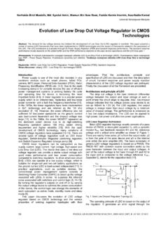
1 486 IEEE JOURNAL OF SOLID-STATE CIRCUITS, VOL. 49, NO. 2, FEBRUARY 2014 External Capacitor-Less Low Drop-Out RegulatorWith 25 dB Superior power supply Rejectionin the 4 MHz RangeChang-Joon Park, Member, IEEE, Marvin Onabajo, Member, IEEE, and Jose Silva-Martinez, Fellow, IEEEA bstract This paper presents design techniques for a highpower supply rejection (PSR) low drop-out (LDO) regulator. Abulky external capacitor is avoided to make the LDO suitablefor system-on-chip (SoC) applications while maintaining thecapability to reduce high -frequency supply noise. The paths ofthe power supply noise to the LDO output are analyzed, and apower supply noise cancellation circuit is developed. The PSRperformance is improved by using a replica circuit that tracksthe main supply noise under process-voltage-temperature varia-tions and all operating conditions. The effectiveness of the PSRenhancement technique is experimentally verified with an LDOthat was fabricated in a m CMOS technology with a powersupply of V.
2 The active core chip area is mm , and theentire proposed LDO consumes 80 A of quiescent current duringoperation mode and 55 A of quiescent current in standby has a drop-out voltage of 200 mV when delivering 50 mA tothe load. The measured PSR is better than 56 dB up to 4 MHzwhen delivering a current of 50 mA. Compared to a conventionaluncompensated LDO, the proposed architecture presents a PSRimprovement of 34 dB and 25 dB at 1 MHz and 4 MHz, Terms External capacitor-less LDO, fast capacitor-lessLDO, high PSR LDO, low drop-out (LDO) regulator, low-noiseLDO, power management, power supply rejection (PSR).I. INTRODUCTIONDUE to the rapidly increasing demand for portable devicessuch as smartphones, tablet PCs and wireless handsets,the use of efficient power management systems to prolongbattery life is becoming of primary importance. With thegrowing trends of complete system-on-chip (SoC) design,the entire power management system should be integratedinto a single-chip solution.
3 The conventional power manage-ment system consists of a highly efficient switching powerconverter (SWPC) cascaded with a low-noise power -efficientlow drop-out (LDO) regulator. To provide good isolationManuscript received April 09, 2013; revised September 10, 2013; acceptedOctober 17, 2013. Date of publication November 26, 2013; date of current ver-sion January 24, 2014. This paper was approved by Associate Editor Eric A. Park was with the Department of Electrical and Computer Engineering,Texas A&M University, College Station, TX 77843 USA. He is now withFreescale Semiconductor Inc., Austin, TX 78735 Silva-Martinez is with the Department of Electrical and Computer Engi-neering, Texas A&M University, College Station, TX 77843 Onabajo is with the Department of Electrical and Computer Engineering,Northeastern University, Boston, MA 02115 versions of one or more of thefigures in this paper are available onlineat Object Identifier the SWPC noisy output and the very noise-sensitiveRF and/or high -performance analog blocks, the LDO s abilityto reject the power supply noise is becoming a very demandingspecification.
4 With the current technology trends, the SWPC operating frequencies are increasing to allow higher levels ofintegration [1]. Since the output ripples at high frequenciesappear at the output of the SWPC, the LDO regulator must havea high power supply rejection (PSR) for frequencies up to afew megahertz with as few off-chip components as possible toreduce die/board area and cost [2]. The issue is complex sincethe supply noise leakage changes with the loading , several techniques to improve the power supplyrejection of LDOs have been proposed [3] [7]. These techniquesinvolve: i) a feed-forward ripple cancellation path employingfixed gain that is not able to track supply noise leakage under alloperating conditions [3] or an adaptive scheme [4], where thepractical feasibility of the approaches is limited because bulkyexternal output capacitors are employed (4F[3]and6F[4]),which improve performance but increase the bill of material in[5] bulk driven techniques are used to improve low-frequencyPSR; ii) a feed-forward supply -noise cancellation (FFNC)method employing calibrationtechniques without an externaloutput capacitor [6], which is an approach that is very sensitiveto the control voltage of the bias current source that determinesthe gain of the feed-forward amplifier hence, it cannot bea robust PSR enhancement solution for the different loadingconditionsunder process-voltage-temperature (PVT)variations.
5 Iii) another technique provides additional isolation employingan NMOS cascade transistor with a clean gate voltage [7].The aforementioned techniques [3] [6] improve the high -fre-quency PSR by cancelling the supply noise induced current be-fore it appears at the load. To provide a suitable solution for SoCapplications, we introduce an external capacitor-less LDO witha PSR enhancement technique that tracks and compensates thesupply noise up to high frequencies without the use of bulky ex-ternal capacitors. It is shown that the leakage of the supply noisehas three main components, and all of them could be tracked;however, in this prototype only the most relevant one in therange 100 KHz 10 MHz is paper is organized as follows. Section II describes thefundamental PSR limitations inconventional LDOs. Section IIIpresents the proposed PSR enhancement technique for whichthe main architecture and circuit implementation of the pro-posed LDO regulator are discussed in Section IV.
6 Measurementresults are provided in Section V, and conclusions are drawn inSection 2013 IEEE. Personal use is permitted, but republication/redistribution requires IEEE for more al.: EXTERNAL CAPACITOR-LESS LOW DROP-OUT REGULATOR WITH 25 dB SUPERIOR power supply REJECTION487II. FUNDAMENTALPSR LIMITATIONSOFCONVENTIONALLDOSLDOs typically have fundamental PSR limitations at highfrequencies due to the existence of several paths between thenoisy supply and the LDO output. Fig. 1 shows those paths fora conventional LDO architecture where supply noise couples tothe output of the LDO as follows: i) Path 1: noise modulationof the gate voltage through the gate-source capacitance,,converted into current by the transconductance of the pass tran-sistor,; ii) Path 2: through the error amplifier; iii) Path 3:noise coupled through thefinite output impedance of the passtransistor,and. For the conventional LDO depicted inFig. 1, the output voltagedue to power supplynoise can be expressed as(1)where,andare the LDOopen-loop supply noise-induced currents due to the Path 1, Path2, and Path 3, respectively.
7 The effects of all thesenoisecomponents are minimized by increasing the magnitude of theloop gain, provided that loop stability can be guaranteed. Theopen-loop schematic of a conventional external capacitor-lessLDO architecture employing a two-stage error amplifier and fre-quency compensation [8], [9] is depicted in Fig. 2(a). To easethe analysis, thefloating capacitoris represented by fourcircuit elements as shown in Fig. 2(b) [10]. The loop gain canthen be expressed as(2)whereis the feedback factor the frequency compensation ca-pacitor for loop stability, which is usually implemented with animpedance scaling technique [8], [9], [11]. For an external ca-pacitor-less LDO, increasing the loop gain can partially alleviatethe PSR degradation at medium and high frequencies. However,this approach may not be very attractive since the design withwide-band loop gain usually results in excessive power con-sumption. To obtain insights into improvement at high frequen-cies, the fundamental PSR limitations due to each supply noisepath are analyzed in more detail in the following PSR Limitations Due to the Gate-Source Capacitance ofthe Pass TransistorAt high frequencies, the pass transistor,,isthemajorfactor that limits the LDO s PSR.
8 As depicted in Fig. 3(a),the gate voltage of transistor, is modulated bythrough the capacitor. The drain current generated byandof transistorappears at the LDO output. Thiscurrent is determined by the voltage difference between sourceand a local feedbackthat makesa function of the output voltage, it complicatesFig. 1. Input-to-output power supply ripple paths in a conventional analysis ofnoise. Following the approach in Fig. 2,this capacitor is split into four components consisting of twogrounded capacitors and two voltage-controlled current sources(VCCS) as depicted in Fig. 3(b). The componentisa local feedback and its effect is embedded in the loop gate-source capacitor is also split into two pieces (the othertwo are attached to, and thus do not affect the analysis),which leads to the grounded capacitor(one of the com-ponents of) and the voltage controlled capacitive currentsource,. Since the pole due to equivalent resistance(K) and gate capacitance (pF) is locatedat a low frequency of approximately 10 KHz, the effect ofcan be ignored for high -frequency analysis.
9 The gate voltage asfunction ofcan be approximated as follows:(3)It is important to remark thatandare much bigger thansince the dimensions ofare much greater than those ofthe other transistors, and thereforecan be ignored in (3).B. PSR Limitations Due to the Error AmplifierMost LDOs employing standard single-ended error ampli-fiers have a limited common-mode and supply noise current mirrors are used for converting the differentialsignal to a single-ended signal, asymmetry presented in the cir-cuit is a major issue of the single-ended error amplifier. The con-ventional two-stage error amplifier is shown in Fig. 4(a). Whena PMOS differential input pair and an NMOS current mirrorload are used as thefirst stage,noise is injected into thecommon-source terminal due tofinite output impedance of thecurrent source, which can be modeled by a resistorandcapacitorconnected from the common-source terminalto the supply node as shown in Fig. 4(b). In the single-endedamplifier, the current is not equally split in the two arms due tounavoidable transistor mismatches in the differential pair.
10 Thisnon-ideality generates a differential current at the output that488 IEEE JOURNAL OF SOLID-STATE CIRCUITS, VOL. 49, NO. 2, FEBRUARY 2014 Fig. 2. (a) Open-loop schematic of a conventional external capacitor-less LDO with frequency compensation for a two-stage error amplifier, and (b) its small-signal equivalent proportional to the injected current that depends on the mis-match factor. Another concern is that the impedance seen atthe sources of the differential pair transistors is different dueto the different loading conditions foreach transistor. Thefi-nite output impedance of the current mirror introduces a sys-tematic error. For the abovementioned reasons, it is advisable touse layout matching techniquesandtooptimizetheLDOper-formanc e based on post-layout simulations with extracted par-asitics. The small-signal model of the error amplifier for PSRanalysis is shown in Fig. 4(b). Assuming that the mismatches ofthe PMOS differential pair and NMOS current mirror are mini-mized by layout matching techniques, the supply noise that ap-pears at the output of thefirst stage in the error amplifier can beapproximated by(4)Even if transistor mismatches are minimized,noise com-ponents can still be identified in (4).