Transcription of Advanced AMS1117 Monolithic 800mA LOW DROPOUT …
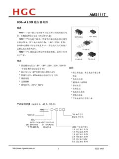
1 Advanced Monolithic Systems, Inc. 6680B Sierra Lane, Dublin, CA 94568 Phone (925) 556-9090 Fax (925) 556-9140 Advanced AMS1117 Monolithic 800mA LOW DROPOUT VOLTAGE REGULATOR SystemsFEATURESAPPLICATIONS Three Terminal Adjustable or Fixed Voltages* High Efficiency Linear Regulators , , , , and Post Regulators for Switching Supplies Output Current of 800mA 5V to Linear Regulator Operates Down to 1V DROPOUT Battery Chargers Line Regulation: Max. Active SCSI Terminators Load Regulation: Max. Power Management for Notebook SOT-223 and TO-252 package available Battery Powered InstrumentationGENERAL DESCRIPTIONThe The AMS1117 series of adjustable and fixed voltage regulators are designed to provide 800mA output current and to operatedown to 1V input-to-output differential. The DROPOUT voltage of the device is guaranteed maximum at maximum outputcurrent, decreasing at lower load currents.
2 On-chip trimming adjusts the reference voltage to 1%. Current limit is also trimmed, minimizing the stress under overloadconditions on both the regulator and power source AMS1117 devices are pin compatible with other three-terminal SCSI regulators and are offered in the low profile surfacemount SOT-223 package and in the TO-252 (DPAK) plastic INFORMATION: PACKAGE TYPEOPERATING JUNCTIONTO-252 SOT-223 TEMPERATURE RANGE AMS1117CD AMS11170 to 125 C to 125 C to 125 C to 125 C to 125 C to 125 C to 125 C*For additional available fixed voltages contact CONNECTIONSFIXED VERSIONADJUSTABLE VERSION1- Ground2- VOUT3- VIN1- Adjust2- VOUT3- VINSOT-223 Top View123 TAB ISOUTPUTTO-252 FRONT VIEW123 Advanced Monolithic Systems, Inc. 6680B Sierra Lane, Dublin, CA 94568 Phone (925) 556-9090 Fax (925) 556-9140 AMS1117 ABSOLUTE MAXIMUM RATINGS (Note 1)Power Dissipation Internally limitedSoldering informationInput Voltage 15V Lead Temperature (10 sec) 300 COperating Junction Temperature RangeThermal Resistance Control Section0 C to 125 C TO-252 package JA= 80 C/W Power Transistor 0 C to 150 C SOT-223 package JA= 90 C/W*Storage temperature- 65 C to +150 C* With package soldering to copper area over backsideground plane or internal power plane JA can vary from46 C/W to >90 C/W depending on mounting technique andthe size of the copper CHARACTERISTICSE lectrical Characteristics at IOUT = 0 mA, and TJ = +25 C unless otherwise Typ MaxUnitsReference Voltage(Note 2) AMS1117 IOUT = 10 mA10mA IOUT 800mA , (VIN - VOUT) Voltage(Note 2)
3 IOUT 800mA , VIN IOUT 800mA , VIN IOUT 800mA , VIN IOUT 800mA , VIN IOUT 800mA , VIN IOUT 800mA , VIN RegulationAMS1117 ILOAD = 10 mA , (VIN - VOUT) VIN VIN VIN VIN VIN VIN Regulation(Notes 2, 3) AMS1117 (VIN - VOUT) =3V, 10mA IOUT = 5V, 0 IOUT = 5V, 0 IOUT = 5V, 0 IOUT 800mA361220mVmVAdvanced Monolithic Systems, Inc. 6680B Sierra Lane, Dublin, CA 94568 Phone (925) 556-9090 Fax (925) 556-9140 AMS1117 ELECTRICAL CHARACTERISTICSE lectrical Characteristics at IOUT = 0 mA, and TJ = +25 C unless otherwise Typ MaxUnitsLoad Regulation(Notes 2, 3) = 5V, 0 IOUT = 5V, 0 IOUT = 8V, 0 IOUT 800mA5102035mVmVDropout Voltage(VIN - VOUT) VOUT , VREF = 1%, IOUT = 800mA (Note 4) (VIN - VOUT) = 5V9001,1001,500mAMinimum LoadCurrentAMS1117(VIN - VOUT) = 12V (Note 5)510mAQuiescent 12V510mARipple RejectionAMS1117f =120Hz , COUT = 22 F Tantalum, IOUT = 800mA ,(VIN-VOUT ) = 3V, CADJ =10 =120Hz , COUT = 22 F Tantalum, IOUT = 800mA ,VIN = =120Hz , COUT = 22 F Tantalum, IOUT = 800mAVIN = =120Hz , COUT = 22 F Tantalum, IOUT = 800mAVIN = 8V6068dBThermal RegulationAMS1117TA = 25 C, 30ms Pin CurrentAMS111710mA IOUT 800mA , (VIN - VOUT) 12V55120 A AAdjust Pin CurrentChangeAMS111710mA IOUT 800mA , (VIN - VOUT)
4 ATemperature Term StabilityTA =125 C, Output Noise(% of VOUT ) TA = 25 C , 10Hz f ResistanceJunction-to-Case15 C/WParameters identified with boldface type apply over the full operating temperature 1: Absolute Maximum Ratings indicate limits beyond which damage to the device may occur. For guaranteed specifications and test conditions, see theElectrical Characteristics. The guaranteed specifications apply only for the test conditions 2: Line and Load regulation are guaranteed up to the maximum power dissipation of W. Power dissipation is determined by the input/output differentialand the output current. Guaranteed maximum power dissipation will not be available over the full input/output 3: See thermal regulation specifications for changes in output voltage due to heating effects. Line and load regulation are measured at a constant junctiontemperature by low duty cycle pulse testing. Load regulation is measured at the output lead ~1/8 from the 4: DROPOUT voltage is specified over the full output current range of the 5: Minimum load current is defined as the minimum output current required to maintain regulation.
5 When (VIN - VOUT) 12V the device isguaranteed to regulate if the output current is greater than Monolithic Systems, Inc. 6680B Sierra Lane, Dublin, CA 94568 Phone (925) 556-9090 Fax (925) 556-9140 AMS1117 APPLICATION HINTSThe AMS1117 series of adjustable and fixed regulators are easyto use and are protected against short circuit and thermaloverloads. Thermal protection circuitry will shut-down theregulator should the junction temperature exceed 165 C at thesense compatible with older three terminal adjustable regulators,these devices offer the advantage of a lower DROPOUT voltage,more precise reference tolerance and improved reference stabilitywith circuit design used in the AMS1117 series requires the use ofan output capacitor as part of the device frequency addition of 22 F solid tantalum on the output will ensurestability for all operating the adjustment terminal is bypassed with a capacitor toimprove the ripple rejection, the requirement for an outputcapacitor increases.
6 The value of 22 F tantalum covers all casesof bypassing the adjustment terminal. Without bypassing theadjustment terminal smaller capacitors can be used with equallygood ensure good transient response with heavy load currentchanges capacitor values on the order of 100 F are used in theoutput of many regulators. To further improve stability andtransient response of these devices larger values of outputcapacitor can be DiodesUnlike older regulators, the AMS1117 family does not need anyprotection diodes between the adjustment pin and the output andfrom the output to the input to prevent over-stressing the resistors are limiting the internal current paths on theAMS1117 adjustment pin, therefore even with capacitors on theadjustment pin no protection diode is needed to ensure devicesafety under short-circuit between the input and output are not usually surge currents of 50A to 100A can be handled by theinternal diode between the input and output pins of the device.
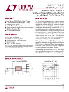
7 Innormal operations it is difficult to get those values of surgecurrents even with the use of large output capacitances. If highvalue output capacitors are used, such as 1000 F to 5000 F andthe input pin is instantaneously shorted to ground, damage canoccur. A diode from output to input is recommended, when acrowbar circuit at the input of the AMS1117 is used (Figure 1).AMS1117IN OUTADJ+COUT22 FVOUTR1R2 CADJ10 FD1 VINF igure VoltageThe AMS1117 series develops a reference voltagebetween the output and the adjust terminal. Placing a resistorbetween these two terminals causes a constant current to flowthrough R1 and down through R2 to set the overall outputvoltage. This current is normally the specified minimum loadcurrent of 10mA. Because IADJ is very small and constant itrepresents a small error and it can usually be OUTADJR1R2 VOUTVREFVINIADJ50 AVOUT = VREF (1+ R2/R1)+IADJR2 Figure 2.
8 Basic Adjustable RegulatorLoad RegulationTrue remote load sensing it is not possible to provide, becausethe AMS1117 is a three terminal device. The resistance of thewire connecting the regulator to the load will limit the loadregulation. The data sheet specification for load regulation ismeasured at the bottom of the package. Negative side sensing is atrue Kelvin connection, with the bottom of the output dividerreturned to the negative side of the best load regulation is obtained when the top of the resistordivider R1 is connected directly to the case not to the load. If R1were connected to the load, the effective resistance between theregulator and the load would be: RP x ( R2+R1 ) , RP = Parasitic Line Resistance R1 Advanced Monolithic Systems, Inc. 6680B Sierra Lane, Dublin, CA 94568 Phone (925) 556-9090 Fax (925) 556-9140 AMS1117 APPLICATION HINTSC onnected as shown , RP is not multiplied by the divider ratioAMS1117IN OUTADJRLR1*R2*VINRPPARASITICLINE RESISTANCE*CONNECT R1 TO CASE CONNECT R2 TO LOADF igure 3.
9 Connections for Best Load Regulation In the case of fixed voltage devices the top of R1 is connectedKelvin internally, and the ground pin can be used for negativeside ConsiderationsThe AMS1117 series have internal power and thermal limitingcircuitry designed to protect the device under overload maximum junction temperature ratings of 125 C shouldnot be exceeded under continuous normal load consideration must be given to all sources of thermalresistance from junction to ambient. For the surface mountpackage SOT-223 additional heat sources mounted near thedevice must be considered. The heat dissipation capability of thePC board and its copper traces is used as a heat sink for thedevice. The thermal resistance from the junction to the tab for theAMS1117 is 15 C/W. Thermal resistance from tab to ambientcan be as low as 30 total thermal resistance from junction to ambient can be aslow as 45 C/W.
10 This requires a reasonable sized PC board withat least on layer of copper to spread the heat across the board andcouple it into the surrounding have shown that the heat spreading copper layerdoes not need to be electrically connected to the tab of the PC material can be very effective at transmitting heatbetween the pad area, attached to the pad of the device, and aground plane layer either inside or on the opposite side of theboard. Although the actual thermal resistance of the PC materialis high, the Length/Area ratio of the thermal resistance betweenlayers is small. The data in Table 1, was taken using 1/16 FR-4board with 1 oz. copper foil, and it can be used as a roughguideline for estimating thermal each application the thermal resistance will be affected bythermal interactions with other components on the board. Todetermine the actual value some experimentation will power dissipation of the AMS1117 is equal to:PD = ( VIN - VOUT )( IOUT )Maximum junction temperature will be equal to:TJ = TA(MAX) + PD(Thermal Resistance (junction-to-ambient))Maximum junction temperature must not exceed 125 RejectionThe ripple rejection values are measured with the adjustment pinbypassed.