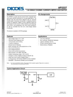
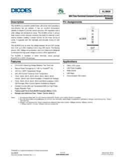
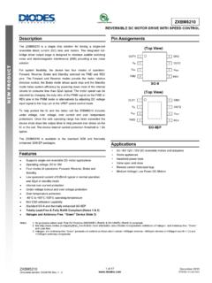
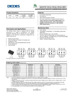
Transcription of AP1509 - Diodes Incorporated
1 AP1509 Document number: DS31016 Rev. 6 - 2 1 of 12 February 2020 Diodes Incorporated AP1509 150kHz, 2A PWM BUCK DC-DC CONVERTER Description The AP1509 series are monolithic ICs designed for a step-down DC-DC converter and have the ability of driving a 2A load without an additional transistor, which saves board space. The external shutdown function can be controlled by logic level and then go into standby mode. The internal compensation makes feedback control have good line and load regulation without external design. Regarding protected function, thermal shutdown prevents overtemperature operating from damage, and current limit works against overcurrent operating of the output switch. If current limit function occurs, and VFB is below , the switching frequency is reduced. The AP1509 series operates at a switching frequency of 150kHz thus allowing smaller-sized filter components than what is required with lower frequency switching regulators.
2 Other features include a guaranteed +4% tolerance on output voltage under specified input voltage and output load conditions, and +15% on the oscillator frequency. The output version included fixed , 5V, 12V, and an adjustable type. The chips are available in a standard 8-lead SO-8 package. Pin Assignments (Top View)12348765 VINGNDFBAP1509 GNDO utputGNDGNDSDSOP-8L Features Output Voltage: , 5V, 12V, and Adjustable Output Version Adjustable Version Output Voltage Range of to 18V+4% 150kHz +15% Fixed Switching Frequency Voltage Mode Non-Synchronous PWM Control Thermal-Shutdown and Current-Limit Protection ON/OFF Shutdown Control Input Operating Voltage up to 22V Output Load Current: 2A Low Power Standby Mode Built-in Switching Transistor On Chip Totally Lead-Free & Fully RoHS Compliant (Note 1 & 2) Halogen and Antimony Free. Green Device (Note 3) For automotive applications requiring specific change control ( parts qualified to AEC-Q100/101/200, PPAP capable, and manufactured in IATF 16949 certified facilities), please contact us or your local Diodes representative.
3 Applications Simple High-Efficiency Step-Down Regulator On-Card Switching Regulators Positive to Negative Converter Notes: 1. No purposely added lead. Fully EU Directive 2002/95/EC (RoHS), 2011/65/EU (RoHS 2) & 2015/863/EU (RoHS 3) compliant. 2. See for more information about Diodes Incorporated s definitions of Halogen- and Antimony-free, "Green" and Lead-free. 3. Halogen- and Antimony-free "Green products are defined as those which contain <900ppm bromine, <900ppm chlorine (<1500ppm total Br + Cl) and <1000ppm antimony compounds. AP1509 Document number: DS31016 Rev. 6 - 2 2 of 12 February 2020 Diodes Incorporated AP1509 Typical Application Circuit (1) Fixed Type Circuit 1284312 VDC InputCINC apacitorFBSDD1 Schottky LoadGNDGNDGND567 (2) Adjustable Type Circuit 1284312 VDC InputCINC apacitorFBSDD1 Schottky LoadGNDGNDGND567R1 1KR2 1K VOUT = VFB (1 +R2R1) VFB = R2 = 1K ~ 3K (3) Delay Start Circuit 1284312 VDC InputCINC apacitorFBSDD1 Schottky LoadGNDGNDGND567R1 1KR2 AP1509 Document number: DS31016 Rev.
4 6 - 2 3 of 12 February 2020 Diodes Incorporated AP1509 Pin Descriptions Functional Block Diagram ++_+_ThermalShutdownPre-driverCompCompGN DO utputVINSDFB220mV200mV2 ASwitch+__AmpCompFrequecy compen- sation Pin Name Description VIN Operating Voltage Input Output Switching Output GND Ground FB Output Voltage Feedback Control SD ON/OFF Shutdown 150kHz OSC. AP1509 Document number: DS31016 Rev. 6 - 2 4 of 12 February 2020 Diodes Incorporated AP1509 Absolute Maximum Ratings Symbol Parameter Rating Unit ESD HBM Human Body Model ESD Protection 2 KV ESD MM Machine Model ESD Protection 200 V VIN Supply Voltage +24 V VSD ON/OFF Pin Input Voltage to +18 V VFB Feedback Pin Voltage to +18 V VOUT Output Voltage to Ground -1 V PD Power Dissipation Internally Limited W TST Storage Temperature -65 to +150 C TJ Operating Junction Temperature -40 to +125 C Recommended Operating Conditions Symbol Parameter Min Max Unit IOUT Output Current 0 2 A VOP Operating Voltage 22 V TA Operating Ambient Temperature -20 85 C AP1509 Document number: DS31016 Rev.
5 6 - 2 5 of 12 February 2020 Diodes Incorporated AP1509 Electrical Characteristics Unless otherwise specified, VIN = 12V for , 5V, adjustable version, and VIN = 18V for the 12V version. ILOAD = Specifications with boldface type are for full operating temperature range, the other type are for TJ = 25 C. Symbol Parameter Conditions Min Typ. Max Unit IFB Feedback Bias Current VFB = (Adjustable Version Only) -10 -50 nA -100 FOSC Oscillator Frequency 127 150 173 kHz 110 173 FSCP Oscillator Frequency of Short Circuit Protect When Current Limit Occurred and VFB < , Ta = 25 C 10 30 50 kHz VSAT Saturation Voltage IOUT = 2A No Outside Circuit VFB = 0V Force Driver On V DC Max. Duty Cycle (ON) VFB = 0V Force Driver On 100 % Min. Duty Cycle (OFF) VFB = 12V Force Driver Off 0 ICL Current Limit Peak Current No Outside Circuit VFB = 0V Force Driver On 3 A IL Output = 0 Output Leakage Current No Outside Circuit VFB = 12V Force Driver Off -200 A Output = -1 VIN = 22V -5 mA IQ Quiescent Current VFB = 12V Force Driver Off 5 10 mA ISTBY Standby Quiescent Current ON/OFF pin = 5V VIN = 22V 70 150 A 200 VIL ON/OFF Pin Logic Input Threshold Voltage Low (Regulator ON) V VIH High (Regulator OFF) IH ON/OFF Pin Logic Input Current VLOGIC = (OFF) A IL ON/OFF Pin Input Current VLOGIC = (ON)
6 -1 JA Thermal Resistance SO-8 Junction to Case 15 C/W JC Thermal Resistance with a Copper Area of Approximately 3in2 SO-8 Junction to Ambient 70 C/W AP1509 - ADJ VFB Output Feedback < VIN < 22V < ILOAD < 2A VOUT Programmed for 3V V Efficiency VIN = 12V, ILOAD=2A 76 76 % AP1509 - VOUT Output Voltage < VIN < 22V < ILOAD < 2A V Efficiency VIN = 12V, ILOAD = 2A 78 78 % AP1509 - 5V VOUT Output Voltage 7V < VIN < 22V < ILOAD < 2A 5 V Efficiency VIN = 12V, ILOAD = 2A 83 83 % AP1509 - 12V VOUT Output Voltage 15V < VIN < 22V < ILOAD < 2A 12 V Efficiency VIN = 15V, ILOAD = 2A 90 90 % AP1509 Document number: DS31016 Rev. 6 - 2 6 of 12 February 2020 Diodes Incorporated AP1509 Typical Performance Characteristics AP1509 Efficiency vs. Temperature (VIN = 12V, VOUT = 5V, Io = 2A) 757677787980818283848586-50-30-101030507 090110130150 Temperature (TA) ( C)Efficiency (%) AP1509 Efficiency vs.
7 Temperature (VIN = 12V, VOUT = , Io = 2A) 737475767778798081-50-30-101030507090110 130150 Temperature (TA) ( C)Efficiency (%) AP1509 Saturation Voltage vs. Temperature (VIN = 12V, VFB = 0V, VSD = 0) (TA) ( C)Saturation Voltage (V) AP1509 Switch Current Limit vs. Temperature (VIN = 12V, VFB = 0V) (TA) ( C)Switch Current Limit (A) AP1509 Supply Current vs. Temperature (VIN = 12V, No Load, Von/off = 0V (Switch ON) ,Von/off = 5V (Switch OFF)) 56789101112131415-50-30-1010305070901101 30150 Temperature (TA) ( C)Supply Current (mA)Switch ON 30354045505560-50-30-1010305070901101301 50 Temperature (TA) ( C)Supply Current (uA)Switch OFF AP1509 Document number: DS31016 Rev. 6 - 2 7 of 12 February 2020 Diodes Incorporated AP1509 Typical Performance Characteristics (continued) AP1509 Threshold Voltage vs. Temperature (VIN = 12V, Io = 100mA) (TA) ( C)Threshold Voltage (V) AP1509 ON/OFF Current vs.
8 ON/OFF Voltage (VIN = 12V) -100-90-80-70-60-50-40-30-20-10010036912 151821ON/OFF Voltage (V)ON/OFF Current (nA) AP1509 Frequency vs. Temperature (VIN = 12V, Io = 500mA, VOUT = 5V) 140145150155160165170-50-30-101030507090 110130150 Temperature (TA) ( C)Frequency (KHz) AP1509 Feedback Current vs. Temperature (VIN = 12V, VOUT = 5V, Vfb = ) -50-40-30-20-10010-50-30-101030507090110 130150 Temperature (TA) ( C)Feedback Current (nA) AP1509 Output Voltage vs. Temperature (VIN = 12V, Io = 2A) (TA) ( C)VOUT (V) AP1509 Document number: DS31016 Rev. 6 - 2 8 of 12 February 2020 Diodes Incorporated AP1509 Typical Performance Characteristics (continued) Header Frequency vs. Temperature Feedback Voltage vs. Temperature (VIN = 15V, VOUT = 5V) 01002003004005006007008009001000-4010601 10 Frequency (KHz)Temperature (oC) Voltage (V)Temperature (oC) Supply Current vs. Temperature (VIN = 15V, VOUT = 5V, lOUT = 0A) Supply Current vs.
9 Supply Voltage (VIN = 15V, VOUT = 5V, lOUT = 0A) Current (mA)Temperature (oC) Current (mA)Supply Voltage (V) Efficiency vs. Output Current (VIN = 15V, VOUT = 5V) Efficiency vs. Output Current (VIN = 15V, VOUT = ) 70758085900204060 Efficiency (%)Output Current (mA) 556575850204060 Efficiency (%)Output Current (mA) AP1509 Document number: DS31016 Rev. 6 - 2 9 of 12 February 2020 Diodes Incorporated AP1509 Functions Description Pin Functions +VIN This is the positive input supply for the IC switching regulator. A suitable input bypass capacitor must be presented at this pin to minimize voltage transients and to supply the switching currents required by the regulator. Ground Circuit ground. Output Internal switch. The voltage at this pin switches between (+VIN - VSAT) and approximately with a duty cycle of approximately VOUT/VIN. To minimize coupling to sensitive circuitry, the PCB copper area connected to this pin should be minimized.
10 Feedback This pin senses the regulated output voltage to complete the feedback loop. SD Allows the switching regulator circuit to be shutdown using logic level signals thus dropping the total input supply current to approximately 150 A. Pulling this pin below a threshold voltage of approximately turns the regulator on, and pulling this pin above (up to a maximum of 18V) shuts the regulator down. If this shutdown feature is not required, the SD pin can be wired to the ground pin. Thermal Considerations The SO-8 package requires a heat sink under most conditions. The size of the heat sink depends on the input voltage, the output voltage, the load current, and the ambient temperature. The AP1509 junction temperature rises above ambient temperature for a 2A load and different input and output voltages. The data for these curves was taken with the AP1509 (SO-8 package) operating as a buck-switching regulator in an ambient temperature of 25 C (still air).
