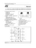
Transcription of Class-AB Speaker Amplifiers 5W+5W Stereo Speaker ... - Rohm
1 1/10 - 2011 ROHM Co., Ltd. All rights reserved. Class-AB Speaker Amplifiers 5W+5W Stereo Speaker Amplifiers BA5406,BA5417 Description The BA5406/BA5417 is a dual OTL monolithic power IC with two built-in, high output Speaker amplifier circuits. High output of 5W 2 can be produced when VCC=12 V and RL=3 , and W 2 when VCC=9V and RL=3 . The BA5406, which uses a high allowable power dissipation package, has a simple heatsink design. The BA5417 not only exceeds basic characteristics, but also has a built-in soft clip circuit, thermal shutdown and standby circuits. Features BA5406 1) Good low voltage characteristics (Operation from Vcc=5 V) 2) Ripple filter (6pin) also can be used as muting pin (Make 6pin GND potential) 3) Small thermal resistance package and simple heatsink design BA5417 1) Small pop noise when standby switches ON/OFF 2) Built-in circuit to prevent ripple addition when motor starts 3) Built-in thermal shutdown circuit 4) Built-in standby switch circuit 5) Built-in soft clip circuit Applications Stereo radio cassette players, mini-audio systems, LCD TVs, etc.
2 Line up matrix Part No. BA5406 BA5417 UnitsSupply voltage 5 ~ 15 6 ~ 15 V Power dissipation 20 15 W Quiescent current 40 22 mA Standby current 0 A Closed loop voltage gain 46 45 dB Output noise voltage mVrmsTotal harmonic distortion % Ripple rejection 55 dB Package SIP-M12 HSIP15 Note 2/10 - 2011 ROHM Co., Ltd. All rights reserved. BA5406,BA5417 Absolute maximum ratings (Ta=25 C) Parameter SymbolRatings Unit BA5406 BA5417 Supply voltage Vcc 18 *1 20 *1 V Power dissipation Pd 20 *2 15 *3 W Operating temperature Topr -20 ~ +75-20 ~ +75 C Storage temperature Tstg -30 ~ +125-55 ~ +150 C *1 When no signal *2 Back metal temperature 75 C *3 Ta=75 C (Using infinite heatsink) Operating range (Ta=25 C) Parameter SymbolRatings Unit BA5406 BA5417 Supply voltage VCC ~ ~ Electrical characteristics (BA5406.)
3 Unless otherwise noted, Ta=25 C, Vcc=12V) (BA5417 : Unless otherwise noted, Ta=25 C, Vcc=9V) Parameter SymbolLimits BA5406 BA5417 Quiescent current IO 40 22 mA VIN=0 Vms Rated output power POUT W THD=10%,Vcc=12V, RL=3 Closed loop voltage gain GVC 46 45 dB Output noise voltage VNO mVrms Rg=10k , DIN-Audio Total harmonic distortion THD % POUT= , f=1kHz Ripple rejection RR 55 dB fRR=100Hz.
4 VRR=-10dBm Crosstalk CT 65 dB VO=0dBm Standby current IOFF 0 A Standby pin input current ISIN mA VSTBY=VCC Standby pin control voltage Activated VSTH ~ VccV Not Activated VSTL 0 ~ V * Note: This IC is not designed to be radiation-resistant. Technical Note 3/10 - 2011 ROHM Co., Ltd. All rights reserved. BA5406,BA5417 Block diagram VccOUTPUT1 BOOT STRAP1 NFB1 INPUT1 FILTERFILTERGNDOUTPUT2 BOOT STRAP2 NFB2 INPUT2 PowerStagePowerStageDriverDriverPreStage PreStageMuting Timer134523456734589101112 BA5406 BA5417 12B SB SS T.
5 B Y3456789101112131415T . S . D-+-+30k30k30k30k4545 VccPOWERGNDPREGND1 PREGND2( )BS2 OUT2 VCCOUT1BS1 POWERGNDSTBYFILTERNF1IN1IN2NF2 PREGND1 PREGND2 FILTERT echnical Note 4/10 - 2011 ROHM Co., Ltd. All rights reserved. BA5406,BA5417 Measurement circuit BA5406 SW: OFF only when measuring IQ BA5417 *1 VSTBY= Technical Note 5/10 - 2011 ROHM Co., Ltd. All rights reserved. BA5406,BA5417 Application circuit BA5406 BA5417 OTL mode circuit BTL mode circuit Technical Note 6/10 - 2011 ROHM Co., Ltd.
6 All rights reserved. BA5406,BA5417 vs frequencyBA5406 Distortion vs Output powerBA5406 Output power vs power supply voltage BA5406 Power dissipation vs Output power(1) BA5406BA5406 Power dissipation vs Output power(2) BA5406 Ripple rejection ratiovs Supply voltageBA5406 Fig. 17 Power dissipation vs Output power(3) Maximum power dissipation vs Supply voltage BA5406 Thermal derating curvewith heat sink without heat sink PCB installed BA5406 Quiescent current and voltage gain vs Supply voltage Voltage gain vs frequencyBA5406 Reference data Distortion vs power supply voltageTechnical Note 7/10 - 2011 ROHM Co.
7 , Ltd. All rights reserved. BA5406,BA5417 BA5417 OTL mode Ripple rejection vs. FrequencyBA5417 Crosstalk vs. Thermal derating curve 010203040506010100100010000100000 FREQUENCY : f (Hz)CLOSED LOOP GAIN : Gvc (dBBA5417 CNF=100 FCNF=47 FCNF=22T=Normal Vcc=9V RL=6 Filter ~10k DIN AUDIO 10k~ WIDE BAND OTL= ( Stereo ) 10 100 1K 10K 100K Closed loop gain vs. Frequency BA5417 Input both channels Rated output power vs Supply voltage BA5417 VOLTAGE : Vcc( V)OUTPUT NOISE VOLTAGE : VNO(mVrms)Rg=10k DIN Output noise voltage vs Supply voltage BA5417 Quiescent, standby pin input current vs.)
8 Supply voltage (Standby pin supply current) BA5417 Power dissipation, circuit current vs. Supply Voltage(RL=4 ) Drive both channels BA5417 Power dissipation, circuit current vs. Supply Voltage RL=8 Drive both channels BA5417 Maximum power dissipation vs. Supply voltage Stereo (OTL) POWER : Po (W)TOTAL HARMONIC DISTORTION : THD(%)BA5417 Vcc=9V RL=3 Input both channels f=100Hz DIN AUDIO 1k DIN AUDIO 10k 200-80k BPF Total harmonic distortion vs Output power 10k1k100(uA) Technical Note 8/10 - 2011 ROHM Co., Ltd. All rights reserved. BA5406,BA5417 010203040506010100100010000100000 FREQUENCY : f(Hz)CLOSED LOOP GAIN : Gvc(dB BA5417 T= Normal Vcc=9V RL=6 VIN=-45dB Heat sink used ( ) 10 100 1K 10K 100K Close loop gain vs.)
9 FrequencyBA5417 BTL mode BA5417 Starting time vs. Input coupling capacitor Normal Input level= T=Normal Vcc=9V RL=6 Input level= 2 7 Icc(A) POWER : Po(W)POWER DISSIPATION : pd(WBA5417T= Normal f=1kHz RL=6 200 HzHPF 20kHzLPF Heat sink used ( ) Pd Icc Vcc=9 VVcc=12 VVcc= Power dissipation, Supply current vs. Frequency BA5417 012345678910024681012141618 POWER SUPPLY : Vcc(V)NEGATIVE FEEDBACK VOLTAGE : VNF1(VF) Output voltage, Negative feed back voltage vs. Supply Voltage BA5417 VNF1 Vout1 Normal temperature RL=6 OUTPUT VOLTAGE : Vcc(V) Normal Ripple rejection vs.)
10 Ripple filter capacitorBA5417 T= Normal Vcc=9V RL=6 VIN=-10dBm 0102030405060708005101520 POWER SUPPLY : Vcc( V)RIPPLE REJECTION : RR(dB)BA5417 Ripple rejection ratio vs. Supply Voltage T= Normal RL=6 f=100Hz Vpp=-10dBm Heat sink used ( ) 20kHzLPF POWER : Po(W)TOTAL HARMONIC DISTORTION : THD (%) .BA5417f=10kHzf=100 Hzf=1kHzT= Normal Vcc=9V RL=6 Heat sink used ( ) Total harmonic distortion vs. Output power Starting time vs. Supply VoltageT= Normal RL=6 VIN= f=1kHz 200 HzHPF 20kHzLPF(RL=6 ) Starting time vs. Ripple filter capacitor BA5417 Output offset voltage vs. Supply Voltage Normal BA5417 Normal Heat sink used ( ) Rated output power vs.