Transcription of Datasheet - production data - st.com
1 June 2016 DocID2145 Rev 26 1/45 This is information on a product in full production . L78L Positive voltage regulators Datasheet - production data Features Output current up to 100 mA Output voltages of ; 5; 6; 8; 9; 10; 12; 15; 18; 24 V thermal overload protection Short-circuit protection No external components are required Available in either 4% (A) or 8% (C) selection Description The L78L series of three-terminal positive regulators employ internal current limiting and thermal shutdown, making them essentially indestructible.
2 If adequate heat-sink is provided, they can deliver up to 100 mA output current. They are intended as fixed voltage regulators in a wide range of applications including local or on-card regulation for elimination of noise and distribution problems associated with single-point regulation. In addition, they can be used with power pass elements to make high-current voltage regulators. The L78L series used as Zener diode/resistor combination replacement, offers e improvement along with lower quiescent current and lower noise. Contents L78L 2/45 DocID2145 Rev 26 Contents 1 Diagram.
3 3 2 Pin configuration .. 4 3 Maximum ratings .. 5 4 Electrical characteristics .. 6 5 Typical performance .. 25 6 Typical application .. 27 7 Package information .. 29 TO-92 package information .. 29 TO-92 packing information .. 30 TO-92 Ammopak packing information .. 32 SO-8 package information .. 34 SO-8 packing information .. 36 SOT-89 package information .. 37 SOT-89 packing 40 8 Ordering information .. 41 9 Revision history .. 44 L78L Diagram DocID2145 Rev 26 3/45 1 Diagram Figure 1: Schematic diagram Pin configuration L78L 4/45 DocID2145 Rev 26 2 Pin configuration Figure 2: Pin connection (top view, bottom view for TO-92) Figure 3: Test circuits L78L Maximum ratings DocID2145 Rev 26 5/45 3 Maximum ratings Table 1.
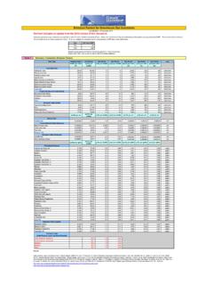
4 Absolute maximum ratings Symbol Parameter Value Unit VI DC Input voltage VO = to 9 V 30 V VO = 12 to 15 V 35 VO = 18 to 24 V 40 IO Output current 100 mA PD Power dissipation Internally limited (1) mW TSTG Storage temperature range -65 to 150 C TOP Operating junction temperature range for L78 LxxAC / L78 LxxC 0 to 125 C for L78 LxxAB -40 to 125 Notes: (1)Our SO-8 package used for voltage regulators is modified internally to have pins 2, 3, 6 and 7 electrically communed to the die attach flag. This particular frame decreases the total thermal resistance of the package and increases its ability to dissipate power when an appropriate area of copper on the printed circuit board is available for heat-sinking.
5 The external dimensions are the same as for the standard SO-8. Table 2: Thermal data Symbol Parameter SO-8 TO-92 SOT-89 Unit RthJC Thermal resistance junction-case (max) 20 15 C/W RthJA Thermal resistance junction-ambient (max) 55 (1) 200 55 (1) C/W Notes: (1)Considering 6 cm of copper Board heat-sink. Electrical characteristics L78L 6/45 DocID2145 Rev 26 4 Electrical characteristics Refer to the test circuits, TJ = 0 to 125 C, VI = V, IO = 40 mA, CI = F, CO = F unless otherwise specified. Table 3: Electrical characteristics of L78L33C Symbol Parameter Test conditions Min.
6 Typ. Max. Unit VO Output voltage TJ = 25 C V VO Output voltage IO = 1 to 40 mA, VI = to 20 V V IO = 1 to 70 mA, VI = V VO Line regulation VI = to 20 V, TJ = 25 C 150 mV VI = to 20 V, TJ = 25 C 100 VO Load regulation IO = 1 to 100 mA, TJ = 25 C 60 mV IO = 1 to 40 mA, TJ = 25 C 30 Id Quiescent current TJ = 25 C 6 mA TJ = 125 C mA Id Quiescent current change IO = 1 to 40 mA mA VI = to 20 V eN Output noise voltage B = 10 Hz to 100 kHz, TJ = 25 C 40 V SVR Supply voltage rejection VI = to V.
7 F = 120 Hz IO = 40 mA, TJ = 25 C 41 49 dB Vd Dropout voltage 2 V L78L Electrical characteristics DocID2145 Rev 26 7/45 Refer to the test circuits, TJ = 0 to 125 C, VI = 10 V, IO = 40 mA, CI = F, CO = F unless otherwise specified. Table 4: Electrical characteristics of L78L05C Symbol Parameter Test conditions Min. Typ. Max. Unit VO Output voltage TJ = 25 C 5 V VO Output voltage IO = 1 to 40 mA, VI = 7 to 20 V V IO = 1 to 70 mA, VI = 10 V VO Line regulation VI = to 20 V, TJ = 25 C 200 mV VI = 9 to 20 V, TJ = 25 C 150 VO Load regulation IO = 1 to 100 mA, TJ = 25 C 60 mV IO = 1 to 40 mA, TJ = 25 C 30 Id Quiescent current TJ = 25 C 6 mA TJ = 125 C mA Id Quiescent current change IO = 1 to 40 mA mA VI = 8 to 20 V eN Output noise voltage B = 10 Hz to 100 kHz, TJ = 25 C 40 V SVR Supply voltage rejection VI = 9 to 20 V.
8 F = 120 Hz IO = 40 mA, TJ = 25 C 40 49 dB Vd Dropout voltage 2 V Electrical characteristics L78L 8/45 DocID2145 Rev 26 Refer to the test circuits, TJ = 0 to 125 C,VI = 14 V, IO = 40 mA, CI = F, CO = F unless otherwise specified. Table 5: Electrical characteristics of L78L08C Symbol Parameter Test conditions Min. Typ. Max. Unit VO Output voltage TJ = 25 C 8 V VO Output voltage IO = 1 to 40 mA, VI = to 20 V V IO = 1 to 70 mA, VI = 12 V VO Line regulation VI = to 20 V, TJ = 25 C 200 mV VI = 11 to 20 V, TJ = 25 C 150 VO Load regulation IO = 1 to 100 mA, TJ = 25 C 80 mV IO = 1 to 40 mA, TJ = 25 C 40 Id Quiescent current TJ = 25 C 6 mA TJ = 125 C mA Id Quiescent current change IO = 1 to 40 mA mA VI = 8 to 20 V eN Output noise voltage B = 10 Hz to 100 kHz, TJ = 25 C 60 V SVR Supply voltage rejection VI = 9 to 20 V.
9 F = 120 Hz IO = 40 mA, TJ = 25 C 36 45 dB Vd Dropout voltage V L78L Electrical characteristics DocID2145 Rev 26 9/45 Refer to the test circuits, TJ = 0 to 125 C, VI = 15 V, IO = 40 mA, CI = F, CO = F unless otherwise specified. Table 6: Electrical characteristics of L78L09C Symbol Parameter Test conditions Min. Typ. Max. Unit VO Output voltage TJ = 25 C 9 V VO Output voltage IO = 1 to 40 mA, VI = to 23 V V IO = 1 to 70 mA, VI = 15 V VO Line regulation VI = to 23 V, TJ = 25 C 250 mV VI = 12 to 23 V, TJ = 25 C 200 VO Load regulation IO = 1 to 100 mA, TJ = 25 C 80 mV IO = 1 to 40 mA, TJ = 25 C 40 Id Quiescent current TJ = 25 C 6 mA TJ = 125 C mA Id Quiescent current change IO = 1 to 40 mA mA VI = 12 to 23 V eN Output noise voltage B = 10 Hz to 100 kHz.
10 TJ = 25 C 70 V SVR Supply voltage rejection VI = 12 to 23 V, f = 120 Hz IO = 40 mA, TJ = 25 C 36 44 dB Vd Dropout voltage V Electrical characteristics L78L 10/45 DocID2145 Rev 26 Refer to the test circuits, TJ = 0 to 125 C, VI = 16 V, IO = 40 mA, CI = F, CO = F unless otherwise specified. Table 7: Electrical characteristics of L78L10C Symbol Parameter Test conditions Min. Typ. Max. Unit VO Output voltage TJ = 25 C 10 V VO Output voltage IO = 1 to 40 mA, VI = to 23 V 9 11 V IO = 1 to 70 mA, VI = 16 V 9 11 VO Line regulation VI = to 23 V, TJ = 25 C 230 mV VI = 13 to 23 V, TJ = 25 C 170 VO Load regulation IO = 1 to 100 mA, TJ = 25 C 80 mV IO = 1 to 40 mA, TJ = 25 C 40 Id Quiescent current TJ = 25 C 6 mA TJ = 125 C mA Id Quiescent current change IO = 1 to 40 mA mA VI = 13 to 23 V eN Output noise voltage B = 10 Hz to 100 kHz.