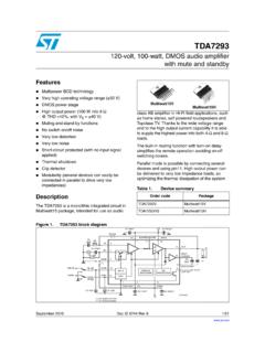
Transcription of Datasheet - TDA2822D - Dual low voltage power amplifier
1 SO8 Features Supply voltage down to V Low crossover distortion Low quiescent current Bridge or stereo configurationDescriptionThe TDA2822D is a monolithic integrated circuit in 8 lead (SO-8) package. It isintended for use as a dual audio power amplifier in portable cassette players, radiosand CD status linkTDA2822 DOrdering informationTDA2822D013 TRDual low voltage power amplifierTDA2822 DDatasheetDS0119 - Rev 3 - August 2020 For further information contact your local STMicroelectronics sales circuitFigure 1. Application circuitFigure 2. Stereo application and test circuitTDA2822 DApplication circuitDS0119 - Rev 3page 2/12 Figure 3.
2 Bridge application and test circuitTDA2822 DApplication circuitDS0119 - Rev 3page 3/122 Pin connectionFigure 4. Pin connectionTDA2822 DPin connectionDS0119 - Rev 3page 4/123 Absolute maximum ratingsTable 1. Absolute maximum ratingsSymbolParameterValueUnitVSSupply voltage15 VIOPeak output1 APtotTotal power dissipation Tamb = 50 and junction temperature-40 to 150 CTjTable 2. Thermal dataSymbolDescriptionValueUnitRthj-ambTh ermal resistance junction-ambient C/WTDA2822 DAbsolute maximum ratingsDS0119 - Rev 3page 5/124 Electrical characteristics(VS = 6 V; Tamb = 25 C, unless otherwise (see Figure 2. Stereo application and test circuit).)
3 Table 3. Electrical characteristics (stereo)SymbolParameterTest conditionsMin. Typ. Max. UnitVSSupply VIdTotal quiescent drain current15 mAVOQ uiescent output = 3 bias current100nAPOO utput power (each channel) (f = 1 kHz, d = 10%)RL = 32 VS= 9 V300mWVS= 6 V120VS = V60VS = 3 V20VS = 2 V5RL = 16 VS = 6 V170 220mWRL = 8 VS = 6 V300 380mWRL = 4 VS = V320mWVS = 3 V110dDistortionRL = 32 PO = 40 PO = 75 = 8 PO = 150 loop voltage gainf = 1 kHz36 39 41 dB GVChannel balance1 dBRiInput resistancef = 1 kHz100k eNTotal input noiseRs = 10 k , B = curve A2 VRs = 10 k , B = 22 Hz to 22 VSVR Supply voltage rejectionf = 100 Hz, C1 = C2 = 100 F24 30dBCsChannel separationf = 1 kHz50dBTDA2822 DElectrical characteristicsDS0119 - Rev 3page 6/12 Bridge (see Figure 3.)
4 Bridge application and test circuit).Table 4. Electrical characteristics (bridge)SymbolParameterTest conditionsMin. Typ. Max. UnitVSSupply VIdTotal quiescent drain currentRL = 15 mAVOSO utput offset voltage between the outputsRL = 8 80 mVIbInput bias current100nAPOO utput power (f = 1 kHz, d = 10%)RL = 32 VS = 9 V1000mWVS = 6 V320400VS = V200VS = 3 V5065VS = 2 V8RL = 16 VS = 6 V800mWVS = 3 V120RL = 8 VS = V700mWVS = 3 V220RL = 4 VS = 3 V350mWVS = 2 V80dDistortionRL = 8 PO = mW, f = 1 loop voltage gainf = 1 kHz39dBRiInput resistancef = 1 kHz100k eNTotal input noiseRs =10 k , B = curve VRs = 10 k , B = 22 Hz to 22 kHz3 SVR Supply voltage rejectionf = 100 Hz40dBBPower bandwidth (-3 dB)
5 RL = 8 k , PO = 1 W120kHzTDA2822 DElectrical characteristicsDS0119 - Rev 3page 7/12 Figure 5. Supply voltage rejection vs. frequencyFigure 6. Output power vs. supply voltage (THD=10%, f=1 kHz stereo)Figure 7. Total power dissipation vs. output power (bridge, RL=8 )Figure 8. Total power dissipation vs. output power (bridge, RL=4 )TDA2822 DElectrical characteristicsDS0119 - Rev 3page 8/125 Package informationIn order to meet environmental requirements, ST offers these devices in different grades of ECOPACK packages,depending on their level of environmental compliance. ECOPACK specifications, grade definitions and productstatus are available at: ECOPACK is an ST package informationFigure 9.
6 SO8 package outlineTable 5. SO-8 mechanical 8 informationDS0119 - Rev 3page 9/12 Revision historyTable 6. Document revision historyDateVersionChanges05-Sep-20031No history because of the ordering information table in cover - Rev 3page 10/12 Contents1 Application maximum package - Rev 3page 11/12 IMPORTANT NOTICE PLEASE READ CAREFULLYSTM icroelectronics NV and its subsidiaries ( ST ) reserve the right to make changes, corrections, enhancements, modifications, and improvements to STproducts and/or to this document at any time without notice. Purchasers should obtain the latest relevant information on ST products before placing orders.
7 STproducts are sold pursuant to ST s terms and conditions of sale in place at the time of order are solely responsible for the choice, selection, and use of ST products and ST assumes no liability for application assistance or the design ofPurchasers license, express or implied, to any intellectual property right is granted by ST of ST products with provisions different from the information set forth herein shall void any warranty granted by ST for such and the ST logo are trademarks of ST. For additional information about ST trademarks, please refer to All other product or servicenames are the property of their respective in this document supersedes and replaces information previously supplied in any prior versions of this document.
8 2020 STMicroelectronics All rights reservedTDA2822 DDS0119 - Rev 3page 12/12
