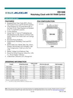
Transcription of DS2M ppm I 2C Real-Time Cloc - Maxim Integrated
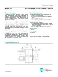
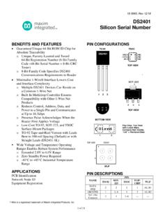
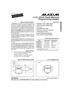
1 DS3231M 5ppm, I2C Real-Time clock General Description Benefits and Features The DS3231M is a low-cost, extremely accurate, I2C real- Highly Accurate RTC With Integrated MEMS. time clock (RTC). The device incorporates a battery input Resonator Completely Manages All Timekeeping and maintains accurate timekeeping when main power to Functions the device is interrupted. The integration of the microelec- Complete clock Calendar Functionality Including tromechanical systems (MEMS) resonator enhances the Seconds, Minutes, Hours, Day, Date, Month, and long-term accuracy of the device and reduces the piece- Year, with Leap-Year Compensation Up to Year part count in a manufacturing line. The DS3231M is avail- 2100. able in the same footprint as the popular DS3231 RTC. Timekeeping Accuracy 5ppm ( Second/Day). The RTC maintains seconds, minutes, hours, day, date, from -45 C to +85 C.
2 Month, and year information. The date at the end of the Footprint and Functionally Compatible to DS3231. month is automatically adjusted for months with fewer Two time -of-Day Alarms than 31 days, including corrections for leap year. The 1Hz and Outputs clock operates in either the 24-hour or 12-hour format Reset Output and Pushbutton Input with Debounce with an AM/PM indicator. Two programmable time -of- Digital Temp Sensor with 3 C Accuracy day alarms and a 1Hz output are provided. Address and + to + Supply Voltage data are transferred serially through an I2C bidirectional Simple Serial Interface Connects to Most bus. A precision temperature-compensated voltage refer- Microcontrollers ence and comparator circuit monitors the status of VCC Fast (400kHz) I2C Interface to detect power failures, to provide a reset output, and to Battery-Backup Input for Continuous Timekeeping automatically switch to the backup supply when neces- Low Power Operation Extends Battery-Backup sary.
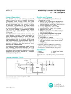
3 Additionally, the RST pin is monitored as a pushbutton Run time input for generating a microprocessor reset. See the Block Diagram for more details. Operating Temperature Range: -40 C to +85 C. 8-Pin or 16-Pin SO Packages Applications Underwriters Laboratories (UL) Recognized Power Meters Industrial Applications Typical Operating Circuit Ordering Information + + PART TEMP RANGE PIN-PACKAGE. DS3231MZ+ -45NC to +85NC 8 SO. DS3231MZ/V+ -45NC to +85NC 8 SO. DS3231M+ -45NC to +85NC 16 SO SCL. I/O PORT. +Denotes a lead(Pb)-free/RoHS-compliant package. SDA. /V denotes an automotive qualified part. 32 KHZ VBAT. INT/SQW. INTERRUPTS. RST. CPU DS3231M. Underwriters Laboratories is a registered certification mark of Underwriters Laboratories Inc. 19-5312; Rev 7; 3/15. DS3231M 5ppm, I2C Real-Time clock Absolute Maximum Ratings Voltage Range on Any Pin Relative to to + Junction +150NC.
4 Operating Temperature -45NC to +85NC Lead Temperature (soldering, 10s)..+300NC. Storage Temperature -55NC to +125NC Soldering Temperature (reflow)..+260NC. Stresses beyond those listed under Absolute Maximum Ratings may cause permanent damage to the device. These are stress ratings only, and functional operation of the device at these or any other conditions beyond those indicated in the operational sections of the specifications is not implied. Exposure to absolute maximum rating conditions for extended periods may affect device reliability. Package Thermal Characteristics (Note 1). 8 SO 16 SO. Junction-to-Ambient Thermal Resistance (qJA)..120 C/W Junction-to-Ambient Thermal Resistance (qJA)..90 C/W. Note 1: Package thermal resistances were obtained using the method described in JEDEC specification JESD51-7, using a four-layer board.
5 For detailed information on package thermal considerations, refer to Recommended Operating Conditions (TA = -45NC to +85NC, unless otherwise noted.) (Note 2). PARAMETER SYMBOL CONDITIONS MIN TYP MAX UNITS. VCC Supply Voltage V. VBAT x VCC +. Logic 1 VIH V. VCC x Logic 0 VIL V. VCC. Electrical Characteristics Frequency And Timekeeping (VCC or VBAT = + , TA = -45NC to +85NC, unless otherwise noted. Typical values are at VCC = + , VBAT = + , and TA = +25NC, unless otherwise noted.). PARAMETER SYMBOL CONDITIONS MIN TYP MAX UNITS. 1Hz Frequency Tolerance Df/fOUT Measured over R 10s interval Q5 ppm 1Hz Frequency Stability vs. VCC. Df/V Q1 ppm/V. Voltage Seconds/. Timekeeping Accuracy tKA Day 32kHz Frequency Tolerance Df/fOUT %. DC Electrical Characteristics General (VCC = + to + , TA = -45NC to +85NC, unless otherwise noted.)
6 Typical values are at VCC = + , VBAT = + , and TA =. +25NC, unless otherwise noted.). PARAMETER SYMBOL CONDITIONS MIN TYP MAX UNITS. Active Supply Current VCC = + 200. (I2C Active: Includes ICCA A. Temperature Conversion Current) VCC = VCCMAX 300. Standby Supply Current VCC = + 130. (I2C Inactive: Includes ICCS A. Temperature Conversion Current) VCC = VCCMAX 200. Temperature Conversion Current VCC = + 575. ICCSCONV A. (I2C Inactive) VCC = VCCMAX 650. Maxim Integrated 2. DS3231M 5ppm, I2C Real-Time clock DC Electrical Characteristics General (continued). (VCC = + to + , TA = -45NC to +85NC, unless otherwise noted. Typical values are at VCC = + , VBAT = + , and TA =. +25NC, unless otherwise noted.). PARAMETER SYMBOL CONDITIONS MIN TYP MAX UNITS. Power-Fail Voltage VPF V. Logic 0 Output VOL IOL = 3mA V. (32 KHZ, INT/SQW, SDA).
7 Logic 0 Output VOL IOL = 1mA V. (RST). Output Leakage ILO + A. (32 KHZ, INT/SQW, SDA). Input Leakage ILI + A. (SCL). RST I/O Leakage IOL -200 +10 A. VBAT Leakage IBATLKG 25 100 nA. Temperature Accuracy TEMPACC VCC or VBAT = + Q3 NC. Temperature Conversion time tCONV 10 ms Pushbutton Debounce PBDB 250 ms Reset Active time tRST 250 ms Oscillator Stop Flag (OSF) Delay tOSF (Note 3) 125 200 ms DC Electrical Characteristics VBAT Current Consumption (VCC = 0V, VBAT = + to + , TA = -45NC to +85NC, unless otherwise noted. Typical values are at VCC = 0V, VBAT = + , and TA = +25NC, unless otherwise noted.). PARAMETER SYMBOL CONDITIONS MIN TYP MAX UNITS. Active Battery Current VBAT = + 70. IBATA A. (I2C Active) (Note 4) VBAT = VBATMAX 150. Timekeeping Battery Current VBAT = + , EN32 KHZ = 0 2 IBATT A. (I2C Inactive) (Note 4) VBAT = VBATMAX, EN32 KHZ = 0 2 Temperature Conversion Current VBAT = + 575.
8 IBATTC A. (I2C Inactive) VBAT = VBATMAX 650. Data Retention Current (Oscillator Stopped and I2C IBATDR TA = +25NC 100 nA. Inactive). AC Electrical Characteristics Power Switch (TA = -45NC to +85NC, unless otherwise noted.) (Figure 2). PARAMETER SYMBOL CONDITIONS MIN TYP MAX UNITS. VCC Fall time , VPFMAX to tVCCF 300 Fs VPFMIN. VCC Rise time , VPFMIN to tVCCR 0 Fs VPFMAX. Recovery at Power-Up tREC (Note 5) 250 300 ms Maxim Integrated 3. DS3231M 5ppm, I2C Real-Time clock AC Electrical Characteristics I2C Interface (VCC or VBAT = + to + , TA = -45NC to +85NC, unless otherwise noted. Typical values are at VCC = + , VBAT = + , and TA = +25NC, unless otherwise noted.) (Note 6, Figure 1). PARAMETER SYMBOL CONDITIONS MIN TYP MAX UNITS. SCL clock Frequency fSCL 0 400 kHz Bus Free time Between STOP. tBUF Fs and START Conditions Hold time (Repeated) START.
9 THD:STA Fs Condition Low Period of SCL tLOW Fs High Period of SCL tHIGH Fs Data Hold time tHD:DAT 0 Fs Data Set-Up time tSU:DAT 100 ns START Set-Up time tSU:STA Fs 20 +. SDA and SCL Rise time tR (Note 7) 300 ns 20 +. SDA and SCL Fall time tF (Note 7) 300 ns STOP Set-Up time tSU:STO Fs SDA, SCL Input Capacitance CBIN (Note 8) 10 pF. Note All voltages are referenced to ground. 2: Note The parameter tOSF is the period of time the oscillator must be stopped for the OSF flag to be set. 3: Note Includes the temperature conversion current (averaged). 4: Note This delay applies only if the oscillator is enabled. If the EOSC bit is 1, tREC is bypassed and RST immediately goes high. 5: The state of RST does not affect the I2C interface or RTC functions. Note 6: I nterface timing shown is for fast-mode (400kHz) operation. This device is also backward-compatible with standard mode I2C timing.
10 Note 7: CB: Total capacitance of one bus line in picofarads. Note 8: Guaranteed by design; not 100% production tested. Maxim Integrated 4. DS3231M 5ppm, I2C Real-Time clock Timing Diagrams SDA. tBUF. tF tSP. tLOW tHD:STA. SCL. tHIGH. tHD:STA tR tSU:STA. tSU:STO. tHD:DAT tSU:DAT. STOP START REPEATED. START. NOTE: TIMING IS REFERENCED TO VILMAX AND VIHMIN. Figure 1. I2C Timing tVCCF tVCCR. VPFMAX. VPFMIN. VCC. tREC. RST. Figure 2. Power Switch Timing RST. PBDB tRST. Figure 3. Pushbutton Reset Timing Maxim Integrated 5. DS3231M 5ppm, I2C Real-Time clock Typical Operating Characteristics (TA = +25 C, unless otherwise noted.). POWER-SUPPLY CURRENT BATTERY-SUPPLY CURRENT. vs. POWER-SUPPLY VOLTAGE vs. BATTERY-SUPPLY VOLTAGE. 150 DS3231M toc01. DS3231M toc02. VBAT = , EN32 KHZ = 1, IOUT = 0mA VCC = 0V, EN32 KHZ = 1, BBSQW = 0.