Transcription of FEBRUARY 2009 REVISED JUNE 2011 Two Output, Integrated …
1 FEBRUARY2009 REVISEDJUNE2011 TwoOutput,IntegratedVCO,Low-JitterClockG eneratorCheckforSamples:CDCM61002 DividerProgrammingUsingControlPins:1 FEATURES TwoPinsforPrescaler/FeedbackDivider2 OneCrystal/LVCMOSR eferenceInput ,25 MHz, TwoPinsforOutputSelect On-ChipVCOO peratesinFrequencyRangeof IndustrialTemperatureRange: 40 C to+85 5-mm 5-mm,32-pin,QFN(RHB)Package 2xOutputAvailable: ESDP rotectionExceeds2 kV(HBM) Pin-SelectableBetweenLVPECL,LVDS,or2-LVC MOS; LVCMOSB ypassOutputAvailable LowJitterClockDriverforHigh-EndDatacom OutputFrequencySelectableby/1,/2,/3,/4,/ 6,ApplicationsIncludingSONET,Ethernet,Fi bre/8froma SingleOutputDividerChannel,SerialATA,and HDTV SupportsCommonLVPECL/LVDSO utput Cost-EffectiveHigh-FrequencyCrystalFrequ encies.
2 OscillatorReplacement , ,75 MHz, ,100 MHz, ,125 MHz,150 MHz, , , , ,200 MHz, ,250 MHz,TheCDCM61002isahighlyversatile, , , ,frequencysynthesizerthatcangeneratetwol ow-jitter625 MHzclockoutputs,selectablebetweenlow-vol tage SupportsCommonLVCMOSO utputpositiveemittercoupledlogic(LVPECL) ,low-voltageFrequencies:differentialsign aling(LVDS),orlow-voltage , ,75 MHz, ,complementarymetaloxidesemiconductor100 MHz, ,125 MHz,150 MHz,(LVCMOS)outputs,froma , , , ,200 MHz, , (SeeTable3) InternalPLLLoopBandwidth:400kHzoutputran domjitterperformanceislessthan1ps,RMS(fr om10kHzto20 MHz),makingthisdevicea High-PerformancePLLCore:perfectchoicefor usein demandingapplicationssuch PhaseNoisetypicallyat 146dBc/HzatasSONET,Ethernet,FibreChannel , availableina small,32-pin,5-mm ,RMS5-mmQFNpackage.
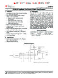
3 (10kHzto20 MHz)for625-MHzLVPECLO utput OutputDutyCycleCorrectedto50%( 5%) LowOutputSkewof20psonLVPECLO utputs1 Pleasebeawarethatanimportantnoticeconcer ningavailability,standardwarranty,anduse in 2009 2011, =INOutput DividerFeedback Divider((fOUTPFDC harge PumpLoop FilterFeedbackDividerPrescalerOutput DividerCELVPECL/LVCMOS/LVDSLVPECL/LVCMOS /LVDSOS[ ]OD[ ]PR[ ] VCDCM61002 Crystal/LVCMOSO utputDriverOutputDriverLVCMOSCDCM61002 SCAS870F FEBRUARY2009 ,CONTINUEDTheCDCM61002isa high-performance,lowphasenoise,fully-int egratedvoltage-controlledoscillator(VCO) ))
4 Clocksynthesizerwithtwouniversaloutputbu ffersthatcanbeconfiguredtobeLVPECL,LVDS, ,anLVCMOS bypassoutputclockis availablein anoutputconfigurationwhichcanhelpwithcry stalloadingin hasonefully- Integrated ,low-noise,LC-base dVCOthatoperatesin (PLL)synchronizestheVCOwithrespecttothei nput, controlpinstructure,whichhastwopinsthatc ontroltheprescalerandfeedbackdivider,thr eepinsthatcontroltheoutputdivider,twopin sthatcontroltheoutputtype, (includingtheinputfrequency,prescalerdiv ider,orfeedbackdivider)arealtered,a resetmustbeissuedthroughtheResetcontrolp in(activelowfordevicereset).
5 Theresetinitiatesa in reset, (fOUT) is proportionaltothefrequencyoftheinputcloc k(fIN). Thefeedbackdivider,outputdivider,andVCOf requencysetfOUTwithrespecttofIN. Fora configurationsettingforcommonwirelineand datacomapplications,refertoTable2. Forotherapplications,useEquation1 tocalculatetheexactcrystaloscillatorfreq uencyrequiredforthedesiredoutput.(1)Theo utputdividercanbechosenfrom1,2,3,4,6,or8 ,24and3,20and4,or15and5,respectively, showsa a characterizedforoperationfrom 40 C to+85 2009 2011, FEBRUARY2009 REVISEDJUNE2011 AVAILABLEOPTIONS(1)TAPACKAGEDDEVICESFEAT URES(2)CDCM61002 RHBT32-pinQFN(RHB)package,smalltapeandre el 40 C to+85 CCDCM61002 RHBR32-pinQFN(RHB)package,tapeandreel(1) Forthemostcurrentspecificationsandpackag einformation, (2)ThesepackagesconformtoLead(Pb).
6 TIdefinesGreentomeanLead(Pb)-Freeandin addition,useslesspackagematerialsthatdon otcontainhalogens,includingbromine(Br),o rantimony(Sb) :NotyetavailableLead(Pb)-Free;forestimat edconversiondates, :TIdefinesLead(Pb)-FreetomeanRoHScompati ble,includinga ,and,if designedtobesoldered,suitableforusein (1)Overoperatingfree-airtemperaturerange (unlessotherwisenoted).PARAMETERVALUEUNI TVCC_OUT,VCC_PLL1,VCC_PLL2,Supplyvoltage range(2) ,VCC_INVINI nputvoltagerange(3) (VCC_IN+ )VVOUTO utputvoltagerange(3) (VCC_OUT+ )VIINI nputcurrent20mAIOUTO utputcurrent50mATSTGS toragetemperaturerange 65to+150 C(1) ,andfunctionaloperationofthedeviceatthes eoranyotherconditionsbeyondthoseindicate dunderrecommendedoperatingconditionis (2)Allsupplyvoltagesmustbesuppliedsimult aneously.
7 (3)Inputandoutputnegativevoltageratingsm aybeexceededif (unlessotherwisenoted). 40+85 CDISSIPATIONRATINGS(1)(2)VALUETEST4 4 VIASPARAMETERCONDITIONSONPADUNIT JAThermalresistance,junction-to-ambient0 LFM35 C/W JP(3)Thermalresistance,junction-to-pad4 C/W(1)Thepackagethermalresistanceis calculatedin accordancewithJESD51andJEDEC2S2P(high-Kb oard).(2)ConnectedtoGNDwithninethermalvi as( ).(3) JP(junction-to-pad)is usedfortheQFNpackage,becausetheprimaryhe atflowis 2009 2011,TexasInstrumentsIncorporated3 CDCM61002 SCAS870F FEBRUARY2009 3 V andTA= 40 C to+85 C, ,VIL= 0 V200 AIILI nputlowcurrentVCC= 3 V,VIH= 200 ALVCMOSO utputCharacteristics(1)(SeeFigure9 andFigure10) mintomax,IOH= 100 AVCC mintomax,IOL= 100 (10kHzto20 MHz) ,RMStSLEW-RATEO utputrise/fallslewrate20%to80% ,fIN= 25 MHz,fOUT= 250 MHz,Devicecurrent,LVCMOS120140mALVCMOSCL = 5 pFLVPECLO utputCharacteristics(2)
8 (SeeFigure11andFigure12) 2 VCC |VOD| (10kHzto20 MHz) ,RMStR/tFOutputrise/falltime20%to80%175p sODCO utputdutycycle45%55%tSKEWS kewbetweenoutputs20psICC,Devicecurrent,L VPECLfIN= 25 MHz,fOUT= 625 MHz126144mALVPECLLVDSO utputCharacteristics(3)(SeeFigure13andFi gure14) |VOD| VOSVOS magnitudechange50mVtRJITRMS phasejitter625 MHz(10kHzto20 MHz) ,RMStR/tFOutputrise/falltime20%to80%255p sODCO utputdutycycle45%55%tSKEWS kewbetweenoutputs30psICC, LVDSD evicecurrent,LVDSfIN= 25 MHz,fOUT= 625 MHz110125mA(1)Figure9 andFigure10showdcandactestsetups, (2)Figure11andFigure12showdcandactestset ups, (3)Figure13andFigure14showdcandactestset ups, 2009 2011, FEBRUARY2009 REVISEDJUNE2011 TYPICALOUTPUTPHASENOISECHARACTERISTICSO veroperatingfree-airtemperaturerange(unl essotherwisenoted).
9 CDCM61002 PARAMETERTESTCONDITIONSMINTYPMAXUNIT250- MHzLVCMOSO utput(1)(seeFigure10)phn100 Phasenoiseat100-Hzoffset 95dBc/Hzphn1kPhasenoiseat1-kHzoffset 110dBc/Hzphn10kPhasenoiseat10-kHzoffset 117dBc/Hzphn100kPhasenoiseat100-kHzoffse t 120dBc/Hzphn1 MPhasenoiseat1-MHzoffset 135dBc/Hzphn10 MPhasenoiseat10-MHzoffset 148dBc/Hzphn20 MPhasenoiseat20-MHzoffset 148dBc/HztRJITRMS phasejitterfrom10kHzto20 MHz544fs, ,PPStart-uptime,powersupplyramptimeof1 ms, 10ppm625-MHzLVPECLO utput(2)(seeFigure12)phn100 Phasenoiseat100-Hzoffset 81dBc/Hzphn1kPhasenoiseat1-kHzoffset 101dBc/Hzphn10kPhasenoiseat10-kHzoffset 109dBc/Hzphn100kPhasenoiseat100-kHzoffse t 112dBc/Hzphn1 MPhasenoiseat1-MHzoffset 129dBc/Hzphn10 MPhasenoiseat10-MHzoffset 146dBc/Hzphn20 MPhasenoiseat20-MHzoffset 146dBc/HztRJITRMS phasejitterfrom10kHzto20 MHz509fs, ,PPStart-uptime,powersupplyramptimeof1 ms, 10ppm625-MHzLVDSO utput(3)(seeFigure14)
10 Phn100 Phasenoiseat100-Hzoffset 88dBc/Hzphn1kPhasenoiseat1-kHzoffset 102dBc/Hzphn10kPhasenoiseat10-kHzoffset 109dBc/Hzphn100kPhasenoiseat100-kHzoffse t 112dBc/Hzphn1 MPhasenoiseat1-MHzoffset 129dBc/Hzphn10 MPhasenoiseat10-MHzoffset 146dBc/Hzphn20 MPhasenoiseat20-MHzoffset 146dBc/HztRJITRMS phasejitterfrom10kHzto20 MHz510fs,RMStPJITT otalperiodjitter27ps,PPStart-uptime,powe rsupplyramptimeof1 ms, 10ppm(1)Figure10showstestsetupanduses25- MHzquartzcrystalin,VCC= ,andTA= +25 C.(2)Figure12showstestsetupanduses25-MHz quartzcrystalin,VCC= ,andTA= +25 C.