Transcription of GaN-based High Efficiency Bidirectional DC-DC Converter ...
1 General rights Copyright and moral rights for the publications made accessible in the public portal are retained by the authors and/or other copyright owners and it is a condition of accessing publications that users recognise and abide by the legal requirements associated with these rights. Users may download and print one copy of any publication from the public portal for the purpose of private study or research. You may not further distribute the material or use it for any profit-making activity or commercial gain You may freely distribute the URL identifying the publication in the public portal If you believe that this document breaches copyright please contact us providing details, and we will remove access to the work immediately and investigate your claim. Downloaded from on: Jan 15, 2021 GaN-based high Efficiency Bidirectional DC-DC Converter with 10 MHz SwitchingFrequencyKruse, Kristian; Zhang, Zhe; Elbo, MadsPublished in:Proceedings of 2017 IEEE Applied Power Electronics Conference and ExpositionPublication date:2017 Document VersionPeer reviewed versionLink back to DTU OrbitCitation (APA):Kruse, K.
2 , Zhang, Z., & Elbo, M. (2017). GaN-based high Efficiency Bidirectional DC-DC Converter with 10 MHzSwitching Frequency. In Proceedings of 2017 IEEE Applied Power Electronics Conference and Exposition high Efficiency Bidirectional DC-DC Converter with 10 MHz Switching Frequency Kristian Kruse, Mads Elbo and Zhe Zhang Dept. Electrical Engineering Technical University of Denmark Kgs. Lyngby, Denmark Abstract Wide bandgap (WBG) semiconductor devices allow power electronic converters to achieve higher Efficiency , higher power density and potentially higher reliability. However, the design challenges accompanied by applying the new WBG devices have risen accordingly. In this paper, a non-isolated Bidirectional DC-DC Converter equipped with Gallium Nitride (GaN) semiconductor transistors is presented. The Converter s operation principles, zero-voltage switching (ZVS) constraints and dead-time effects are studied.
3 Moreover, the optimization and tradeoffs on the adopted high -frequency inductor are investigated. based on the theoretical analysis and calculation, a laboratory prototype with a switching frequency up to 10 MHz and the maximum output power of 100 W is constructed and tested. Switching at 10 MHz, a power density of approximately and an Efficiency of in the Buck mode are achieved. Moreover, the measured losses can match the theoretically calculated counterparts well, therefore the design and analysis are verified. However, from the experimental test carried out, it can also be seen, that making a compact Converter , even for a GaN-based one, operate at 10 MHz and 100 W is still very challenging due to complex ZVS control, lacks of feasible magnetic materials, and limited thermal dissipation area. Keywords Bidirecioinal; Converter ; DC-DC ; dead-time; Gallium Nitride; high switching frequency; soft-switching I.
4 INTRODUCTION Bidirectional DC-DC converters, which can effectively interface energy storage devices such as batteries, supercapacitors and reversible fuel cells to power conversion systems within applications of electrical vehicles (EVs), renewable energy generation (REG), uninterruptible power supplies (USPs) etc., have gained increasing attention in academia and industry over the last decade [1]-[3]. Moreover, with the emergence of applying wide bandgap devices such as Silicon Carbide (SiC) and Gallium Nitride (GaN) based power switches, power electronic converters tend to be even faster, smaller and more efficient, due to the increased electrical field strength and electron mobility compared to than their silicon (Si) based counterparts [4]-[9]. A high switching frequency, to some extent, can certainly offer opportunities for Converter volume reduction and thereby obtain higher power density and more compact design.
5 However, it is also accompanied by new challenges, for instance, increased switching losses even with wide bandgap devices, worse electromagnetic interference (EMI) and more stress on magnetic components [10], [11]. Therefore, soft-switching technologies, including zero-voltage switching (ZVS) and zero-current switching (ZCS), are still widely used in the field of applications of wide band-gap semiconductors. high -frequency soft-switching GaN-based implementations under boundary conduction mode (BCM) have been reported in the literature, in which the reduction of switching loss can well compensate for the increased conduction loss [12]. For instance, a 5-MHz ZVS Boost Converter with the Efficiency up to 98% was demonstrated in [13]; A ZVS extension method is presented based on synchronous rectification in [14] in which a negative inductor current to discharge the switching node capacitance and can achieve ZVS independently from the Converter input to output voltage ratio.
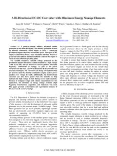
6 In [15], a non-inverting Buck-Boost Converter , as shown in Fig. 1, was proposed, and it is able to achieve full ZVS operation, as well as flexible and easy control, which is significantly better than the resonant converters such as Class-E DC-DC converters. This paper presents a high switching frequency GaN-based Bidirectional DC-DC Converter which can achieve high Efficiency and high power density by a proper design, in particular selecting the optimum dead time. It is shown that the conduction loss increases accordingly when the dead time is longer than the needed ZVS commutation time due to a larger forward voltage drop of GaN devices, thus setting up ideal switching conditions for GaN devices are more severe than their Si counterparts. The paper is organized as follows. After this introduction, the operating principles of the non-inverting Bidirectional Buck-Boost Converter are given Section II.
7 Then, the ZVS constraints with respect to circuit parameters and the dead time effects on the Converter Efficiency are discussed in Fig. 1. Topology of the non-inverting Buck-Boost Converter Fig. 2. Equivalent circuits under different operating modes. (a) (b) Fig. 3. Equivalent circuits under different operating modes. (a) Buck mode; (b) Boost mode. Section III. The design and the corresponding laboratory prototype of the GaN-based Converter with a switching frequency of 10 MHz are presented in Section IV. Finally, the conclusion is given in Section V. II. OPERATION MODES OF THE Bidirectional Converter The non-inverting Buck-Boost Converter consists of four switches, S1~S4 and one inductor L and its topology is depicted in Fig. 1. Basically, the Converter can operate in three modes Buck mode, Boost mode and Buck-Boost mode, depending on the input and output voltage [16], as illustrated in Fig.
8 2. S1 and S2, S3 and S4 always have complementary driving signals with a certain dead-time, tdd, respectively, no matter the operating modes. In the Buck mode, S1 and S2 are regulated by a duty cycle, and S3 and S4 do not operate at the switching frequency, as illustrated in Fig. 3 (a). The low side MOSFET S1 works as a synchronous rectifier and can achieve soft switching, nevertheless, the high side one S2 is hard switched. On the other hand, as shown in (b), during the Boost mode, S3 and S4 operate at the switching frequency and adjusting their duty cycle can convert the voltage between V1 and V2. S4 turns on under zero voltage. When the voltages V1 Fig. 4. Typical waveforms of zero-voltage operation. Fig. 5. Zero voltage commutation between high side and low side switches. and V2 are very close to each other, the Converter must work in the Buck-Boost mode in order to avoid the duty cycle too close to either 1 or zero, which means the Buck-Boost mode is a short transition period between Buck and Boost modes to ensure the smooth and efficient operation within the entire input and output voltage range.
9 Switches S1 and S4, as well as S2 and S3, turn ON and OFF simultaneously. S2 and S3 are soft switched, but the other two switches suffer from turn-on switching loss. III. ZERO-VOLTAGE SWITCHING CONSTRAINTS AND DEADTIME EFFECTS Due to the superior switching performance of wide bandgap devices, adopting them in power converters is accordingly able to reduce switching losses. However, switching losses will still limit the maximum allowed switching frequency within MHz range even for GaN- or SiC- based converters. Moreover, without soft switching, the fast transitions during commutation can cause severe EMI issues which result in rather large filters needed and therefore a bulky and lossy Converter . The mechanism for achieving zero-voltage turn-on is, before the switch is triggered, to completely discharge its output capacitance, which means its anti- paralleled or body diode conducts and thereby can clamp the voltage to almost zero in most cases.
10 The analysis is given based on the Buck operation. However, the same principles can apply to Boost mode and Buck-Boost mode as well. As the waveforms illustrated in Fig. 4, at t2, the low side switch S1 is turned OFF, and in order to discharge Coss_2 to zero voltage, the inductor current must be reversed or negative, as the equivalent circuits illustrated in Fig. 5. Moreover, the energy stored in the inductor at the commutating moment must satisfy: Transition of S2 Transition of S1 Fig. 6. Minimum IL_R as a function of output capacitance and dead time. Dead time (ns)5 101520253035024681012 InductanceCout= 300 pFCout= 200 pFCout= 100 pF Fig. 7. Inductance needed as a function of dead time at V1=100 V. 22_2_21_1_2121 DSossDSossLVCVCE . (1) where EL, Coss_i, i=1,2, and VDS_i, i=1,2 represent energy stored in the inductor L, output capacitance of the switches, and voltage across the switches, respectively.