Transcription of High-speed CAN transceiver - NXP
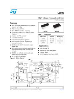
1 1. General descriptionThe TJA1051 is a High-speed CAN transceiver that provides an interface between a Controller Area Network (CAN) protocol controller and the physical two-wire CAN bus. The transceiver is designed for High-speed CAN applications in the automotive industry, providing differential transmit and receive capability to (a microcontroller with) a CAN protocol TJA1051 belongs to the third generation of High-speed CAN transceivers from NXP Semiconductors, offering significant improvements over first- and second-generation devices such as the TJA1050.
2 It offers improved ElectroMagnetic Compatibility (EMC) and ElectroStatic Discharge (ESD) performance, and also features: Ideal passive behavior to the CAN bus when the supply voltage is off TJA1051T/3 and TJA1051TK/3 can be interfaced directly to microcontrollers with supply voltages from 3 Vto5 VThe TJA1051 implements the CAN physical layer as defined in ISO 11898-2:2016 and SAE J2284-1 to SAE J2284-5. This implementation enables reliable communication in the CAN FD fast phase at data rates up to 5 features make the TJA1051 an excellent choice for all types of HS-CAN networks, in nodes that do not require a standby mode with wake-up capability via the Features and General ISO 11898-2.
3 2016 and SAE J2284-1 to SAE J2284-5 compliant Timing guaranteed for data rates up to 5 Mbit/s in the CAN FD fast phase Suitable for 12 V and 24 V systems Low ElectroMagnetic Emission (EME) and high ElectroMagnetic Immunity (EMI) VIO input on TJA1051T/3 and TJA1051TK/3 allows for direct interfacing with 3 V to 5 V microcontrollers (available in SO8 and very small HVSON8 packages respectively) EN input on TJA1051T/E allows the microcontroller to switch the transceiver to a very low- current Off mode Available in SO8 package or leadless HVSON8 package ( mm mm) with improved Automated Optical Inspection (AOI) capability Dark green product (halogen free and Restriction of Hazardous Substances (RoHS) compliant) AEC-Q100 qualifiedTJA1051 High-speed CAN transceiverRev.
4 9 28 November 2017 Product data sheetTJA1051 All information provided in this document is subject to legal disclaimers. NXP 2017. All rights data sheetRev. 9 28 November 2017 2 of 25 NXP SemiconductorsTJA1051 High-speed CAN Low-power management Functional behavior predictable under all supply conditions transceiver disengages from the bus when not powered up (zero load) Protection high ElectroStatic Discharge (ESD) handling capability on the bus pins Bus pins protected against transients in automotive environments Transmit Data (TXD) dominant time-out function Undervoltage detection on pins VCC and VIO Thermally protected3.
5 Quick reference data 4. Ordering information Table reference dataSymbolParameterConditionsMinTypMaxUn itVCCsupply voltage on pin (VCC)undervoltage detection voltage on pin (VIO)undervoltage detection voltage on pin currentSilent mode; bus mode; bus dominant205070mAIIO supply current on pin VION ormal/Silent moderecessive; VTXD=VIO-80250 Adominant; VTXD= 0 V-350500 AVESD electrostatic discharge voltageIEC 61000-4-2 at pins CANH and CANL 8- +8kVVCANH voltage on pin CANH 58-+58 VVCANL voltage on pin CANL 58-+58 VTvjvirtual junction temperature 40-+150 CTable informationType numberPackage NameDescriptionVersionTJA1051 TSO8plastic small outline package; 8 leads; body width mmSOT96-1 TJA1051 All information provided in this document is subject to legal disclaimers.
6 NXP 2017. All rights data sheetRev. 9 28 November 2017 3 of 25 NXP SemiconductorsTJA1051 High-speed CAN transceiver [1]TJA1051T/3 and TJA1051TK/3 with VIOpin; TJA1051T/E with EN Block diagram TJA1051T/3[1]SO8plastic small outline package; 8 leads; body width mmSOT96-1 TJA1051T/E[1]SO8plastic small outline package; 8 leads; body width mmSOT96-1 TJA1051TK/3[1]HVSON8plastic thermal enhanced very thin small outline package; no leads; 8 terminals; body 3 3 mmSOT782-1 Table information ..continuedType numberPackage NameDescriptionVersion(1) In a transceiver without a VIO pin, the VIO input is internally connected to VCC.
7 (2) Only present in the TJA1051 diagramTEMPERATUREPROTECTIONTIME-OUTMODE CONTROLDRIVERTXD1VI/O(1)S8EN(2)5 RXD4 SLOPECONTROL ANDDRIVERVCCCANHCANL76532 GNDTJA1051015aaa036 VCCVIO(1)TJA1051 All information provided in this document is subject to legal disclaimers. NXP 2017. All rights data sheetRev. 9 28 November 2017 4 of 25 NXP SemiconductorsTJA1051 High-speed CAN transceiver6. Pinning Pinning Pin description [1]HVSON8 package die supply ground is connected to both the GND pin and the exposed center pad. The GND pin must be soldered to board ground.
8 For enhanced thermal and electrical performance, it is recommended that the exposed center pad also be soldered to board TJA1051T: SO8b. TJA1051T/E: SO8c. TJA1051T/3: SO8d. TJA1051TK/3: HVSON8 Fig configuration diagrams7;'6*1'&$1+9 'Q F DDD 7-$ 77;'6*1'&$1+9 '(1 DDD 7-$ 7 (7;'6*1'&$1+9 '9,2 DDD 7-$ 7 5;' 9 ' 9,2 &$1/ &$1+ 6 DDD 7-$ 7. WHUPLQDO LQGH[ DUHD7 UDQVSDUHQW WRS YLHZT able descriptionSymbolPinDescriptionTXD1trans mit data inputGND[1]2groundVCC3supply voltageRXD4receive data output; reads out data from the bus connected; in TJA1051T versionEN5enable control input; TJA1051T/E onlyVIO5supply voltage for I/O level adapter; TJA1051T/3 and TJA1051TK/3 onlyCANL6 LOW-level CAN bus lineCANH7 high -level CAN bus lineS8 Silent mode control inputTJA1051 All information provided in this document is subject to legal disclaimers.))]
9 NXP 2017. All rights data sheetRev. 9 28 November 2017 5 of 25 NXP SemiconductorsTJA1051 High-speed CAN transceiver7. Functional descriptionThe TJA1051 is a High-speed CAN stand-alone transceiver with Silent mode. It combines the functionality of the TJA1050 transceiver with improved EMC and ESD handling capability. Improved slope control and high DC handling capability on the bus pins provides additional application TJA1051 is available in three versions, distinguished only by the function of pin 5: The TJA1051T is backwards compatible with the TJA1050 The TJA1051T/3 and TJA1051TK/3 allow for direct interfacing to microcontrollers with supply voltages down to 3 V The TJA1051T/E allows the transceiver to be switched to a very low- current Off Operating modesThe TJA1051 supports two operating modes, Normal and Silent, which are selected via pin S.
10 An additional Off mode is supported in the TJA1051T/E via pin EN. See Ta b l e 4 for a description of the operating modes under normal supply conditions. [1]Only available on the TJA1051T/E.[2]LOW if the CAN bus is dominant, high if the CAN bus is recessive.[3] X = don t Normal modeA LOW level on pin S selects Normal mode. In this mode, the transceiver is able to transmit and receive data via the bus lines CANH and CANL (see Figure 1 for the block diagram). The differential receiver converts the analog data on the bus lines into digital data which is output to pin RXD.