Transcription of High Speed LDO Regulators, Low ESR Cap
1 V14 Page 1 of 20 ME6211 high Speed LDO Regulators, high PSRR, Low noise, ME6211 Series General Description Features The ME6211 series are highly accurate, low noise, CMOS LDO Voltage Regulators. Offering low output noise, high ripple rejection ratio, low dropout and very fast turn-on times, the ME6211 series is ideal for today s cutting edge mobile phone. Internally the ME6211 includes a reference voltage source, error amplifiers, driver transistors, current limiters and phase compensators.
2 The ME6211 s current limiters' foldback circuit also operates as a short protect for the output current limiter and. the output pin. The ME6211 series is also fully compatible with low ESR ceramic capacitors, reducing cost and improving output stability. This high level of output stability is maintained even during frequent load fluctuations, due to the excellent transient response performance and high PSRR achieved across a broad range of CE function allows the output of regulator to be turned off, resulting in greatly reduced power consumption. Maximum Output Current: 500mA VIN ,VOUT Dropout Voltage: 100mV@ IOUT =100mA Operating Voltage Range: 2V Highly Accuracy: 2 Low Power Consumption: 40uA TYP.
3 Standby Current: TPY. high Ripple Rejection: 70dB@1 KHz ME6211C33 Low output noise: 50uVrms Line Regulation: TYP. Package 3-pin SOT89-3 SOT23-3 5-pin SOT23-5 SOT353 6-pin DFN2*2-6L Typical Application Mobile phones Cordless phones, radio communication equipment Portable games Cameras, Video cameras Reference voltage sources Battery powered equipment ME6211 V14 Page 2 of 20 Typical Application Circuit Fig1.
4 ME6211A series Fig2. ME6211C series Fig3. ME6211H series ME6211 V14 Page 3 of 20 Selection Guide Specific voltage and package form pictured above product series product function Output voltage Package ME6211A12PG Enable the internal connection of high SOT89-3 ME6211C33M5G Enable can be set SOT23-5 ME6211H33M5G Enable connected to a low SOT23-5 ME6211 V14
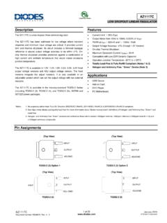
5 Page 4 of 20 Pin Configuration Pin Assignment ME6211 AXXG Pin Number Pin Name Functions M3 P P1 SOT23-3 SOT89-3 SOT89-3 1 1 2 VSS Ground 2 3 1 VOUT Output 3 2 3 VIN Power Input The difference of printing on the chip between P and P1 is : P: , P1: ME6211 AXXG-DS Pin Number Pin Name Functions SOT23-3 1 VIN Power Input 2 VOUT Output 3 VSS Ground ME6211 CXXG/ ME6211 HXXG Pin Number Pin Name Functions SOT23-5/SOT353 DFN2*2-6L 1 3 VIN Power Input 2 2 VSS Ground 3 1 CE ON / OFF Control 4 5,6 NC No Connect 5 4 VOUT Output ME6211 V14 Page 5 of 20 Block Diagram Absolute Maximum Ratings Parameter Symbol Ratings Units Input Voltage VIN V Output Current IOUT 600 mA Output Voltage VOUT VIN + V CE Pin Voltage VCE VIN + V Power Dissipation SOT23 PD 300 mW SOT353 250 DFN2*2-6L 300 SOT89 500 Operating Temperature Range TOPR 40 150 C Storage Temperature Range TSTG 40 150 C
6 ME6211 V14 Page 6 of 20 Electrical Characteristics ME6211C12 (VIN= VOUT+1V VCE = VIN CIN=CL=1uF Ta=25OC ,unless otherwise noted) Parameter Symbol Conditions Min. Typ. Max. Units Output Voltage VOUT(E) (Note 2) IOUT=30mA, VIN= VOUT+1V X VOUT (T) (Note 1) X V Maximum Output Current IOUTMAX VIN= VOUT+1V 300 mA Load Regulation VOUT VIN= VOUT+1V , 1mA IOUT 100mA 8 mV Dropout Voltage (Note 1) VDIF1 IOUT =100mA 280 mV VDIF2 IOUT =200mA 500 mV Supply Current ISS VIN= VOUT+1V 40 A Stand-by Current ICEL VCE 0V A Line Regulation VOUT VIN VOUT IOUT =40mA VOUT+1V VIN %/V CE high Voltage VCEH Start up V CE Low Voltage VCEL Shut down V Output noise EN IOUT =40mA 300Hz~50kHz 50 uVrms Ripple Rejection Rate PSRR VIN = [VOUT +1]V +1Vp-pAC IOUT=10mA, 1kHZ 70 dB IOUT=100mA,10kHZ 62 ME6211C18 (VIN= VOUT+1V VCE = VIN CIN=CL=1uF Ta=25OC, unless otherwise noted) Parameter Symbol Conditions Min.
7 Typ. Max. Units Output Voltage VOUT(E) (Note 2) IOUT=30mA, VIN= VOUT+1V X VOUT (T) (Note 1) X V Maximum Output Current IOUTMAX VIN= VOUT+1V 300 mA Load Regulation VOUT VIN= VOUT+1V , 1mA IOUT 100mA 9 mV Dropout Voltage (Note 1) VDIF1 IOUT =100mA 200 mV VDIF2 IOUT =200mA 400 mV Supply Current ISS VIN= VOUT+1V 40 A Stand-by Current ICEL VCE 0V A Line Regulation VOUT VIN VOUT IOUT =40mA VOUT+1V VIN %/V CE high Voltage VCEH Start up V CE Low Voltage VCEL Shut down V Output noise EN IOUT =40mA 300Hz~50kHz 50 uVrms Ripple Rejection Rate PSRR VIN = [VOUT +1]V+1Vp-pAC IOUT=10mA, 1kHZ 70 dB IOUT=100mA,10kHZ 62 ME6211 V14 Page 7 of 20 ME6211C25 (VIN= VOUT+1V VCE = VIN CIN=CL=1uF Ta=25OC, unless otherwise noted) Parameter Symbol Conditions Min.
8 Typ. Max. Units Output Voltage VOUT(E) (Note 2) IOUT=30mA, VIN= VOUT+1V X VOUT (T) (Note 1) X V Maximum Output Current IOUTMAX VIN= VOUT+1V 400 mA Load Regulation VOUT VIN= VOUT+1V , 1mA IOUT 100mA 9 mV Dropout Voltage (Note 1) VDIF1 IOUT =100mA 110 mV VDIF2 IOUT =200mA 220 mV Supply Current ISS VIN= VOUT+1V 40 A Stand-by Current ICEL VCE 0V 0 A Line Regulation VOUT VIN VOUT IOUT =40mA VOUT+1V VIN %/V CE high Voltage VCEH Start up V CE Low Voltage VCEL Shut down V Output noise EN IOUT =40mA 300Hz~50kHz 50 uVrms Ripple Rejection Rate PSRR VIN=[VOUT+1]V+1Vp-pAC IOUT=10mA, 1kHZ 70 dB IOUT=100mA, 10kHZ 62 IOUT=200mA, 10kHZ 62 Short-circuit Current ISHORT VIN= VOUT+1V, VCE VIN, VOUT 0V 120 mA ME6211C28 (VIN= VOUT+1V VCE = VIN CIN=CL=1uF Ta=25OC, unless otherwise noted) Parameter Symbol Conditions Min.
9 Typ. Max. Units Output Voltage VOUT(E) (Note 2) IOUT=30mA, VIN= VOUT+1V X VOUT (T) (Note 1) X V Maximum Output Current IOUTMAX VIN= VOUT+1V 450 mA Load Regulation VOUT VIN= VOUT+1V , 1mA IOUT 100mA 7 mV Dropout Voltage (Note 1) VDIF1 IOUT =100mA 110 mV VDIF2 IOUT =200mA 220 mV Supply Current ISS VIN= VOUT+1V 50 A Stand-by Current ICEL VCE 0V 0 A Line Regulation VOUT VIN VOUT IOUT =40mA VOUT+1V VIN %/V CE high Voltage VCEH Start up V CE Low Voltage VCEL Shut down V Output noise EN IOUT =40mA 300Hz~50kHz 50 uVrms Ripple Rejection Rate PSRR VIN=[VOUT+1]V+1Vp-pAC IOUT=10mA, 1kHZ 70 dB IOUT=100mA, 10kHZ 62 ME6211 V14 Page 8 of 20 IOUT=200mA, 10kHZ 62 Short-circuit Current ISHORT VIN= VOUT+1V, VCE VIN, VOUT 0V 120 mA ME6211C30 (VIN= VOUT+1V VCE = VIN CIN=CL=1uF Ta=25OC, unless otherwise noted) Parameter Symbol Conditions Min.
10 Typ. Max. Units Output Voltage VOUT(E) (Note 2) IOUT=30mA, VIN= VOUT+1V X VOUT (T) (Note 1) X V Maximum Output Current IOUTMAX VIN= VOUT+1V 500 mA Load Regulation VOUT VIN= VOUT+1V , 1mA IOUT 100mA 8 mV Dropout Voltage (Note 1) VDIF1 IOUT =100mA 100 mV VDIF2 IOUT =200mA 210 mV Supply Current ISS VIN= VOUT+1V 60 A Stand-by Current ICEL VCE 0V 0 A Line Regulation VOUT VIN VOUT IOUT =40mA VOUT+1V VIN %/V CE high Voltage VCEH Start up V CE Low Voltage VCEL Shut down V Output noise EN IOUT =40mA 300Hz~50kHz 50 uVrms Ripple Rejection Rate PSRR VIN = [VOUT +1]V +1Vp-pAC IOUT=10mA, 1kHZ 70 dB IOUT=100mA, 10kHZ 62 IOUT=200mA, 10kHZ 62 Short-circuit Current ISHORT VIN= VOUT+1V, VCE VIN, VOUT 0V 120 mA ME6211C33 (VIN= VOUT+1V VCE = VIN CIN=CL=1uF Ta=25OC, unless otherwise noted) Parameter Symbol Conditions Min.