Transcription of High-Voltage, High-Current OPERATIONAL AMPLIFIER
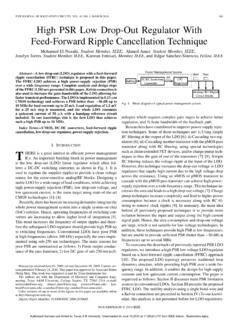
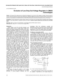
1 OPA548 VIN VIN+V+E/SRCLRCL sets the current limitvalue from 0 to 5A.(1/4W Resistor)ILIMVOV high - voltage , high -CurrentOPERATIONAL AMPLIFIERDESCRIPTIONThe OPA548 is a low-cost, high - voltage / High-Current opera-tional AMPLIFIER ideal for driving a wide variety of loads. Alaser-trimmed monolithic integrated circuit provides excellentlow-level signal accuracy and high output voltage and OPA548 operates from either single or dual supplies fordesign flexibility. In single- supply operation, the input com-mon-mode range extends below OPA548 is internally protected against over-temperatureconditions and current overloads. In addition, the OPA548was designed to provide an accurate, user-selected currentlimit. Unlike other designs which use a power resistor inseries with the output current path, the OPA548 senses theload indirectly. This allows the current limit to be adjustedfrom 0A to 5A with a resistor/potentiometer or controlleddigitally with a voltage -out or current -out Enable/Status (E/S) pin provides two functions.
2 An inputon the pin not only disables the output stage to effectivelydisconnect the load, but also reduces the quiescent currentto conserve power . The E/S pin output can be monitored todetermine if the OPA548 is in thermal OPA548 is available in an industry-standard7-lead staggered and straight lead TO-220 package, and a7-lead DDPAK surface-mount plastic power package. Thecopper tab allows easy mounting to a heat sink or circuitboard for excellent thermal performance. It is specified foroperation over the extended industrial temperature range, 40 C to +85 C. A SPICE macromodel is available fordesign WIDE supply RANGES ingle supply : +8V to +60 VDual supply : 4V to 30V high OUTPUT current :3A Continuous5A Peak WIDE OUTPUT voltage SWING FULLY PROTECTED:Thermal ShutdownAdjustable current Limit OUTPUT DISABLE CONTROL THERMAL SHUTDOWN INDICATOR high SLEW RATE: 10V/ s LOW QUIESCENT current PACKAGES:7-Lead TO-220, Zip and Straight Leads7-Lead DDPAK Surface-MountAPPLICATIONS VALVE, ACTUATOR DRIVERS SYNCHRO, SERVO DRIVERS power SUPPLIES TEST EQUIPMENT TRANSDUCER EXCITATION AUDIO AMPLIFIERSOPA548 SBOS070B OCTOBER 1997 OCTOBER DATA information is current as of publication conform to specifications per the terms of Texas Instrumentsstandard warranty.
3 Production processing does not necessarily includetesting of all 1997-2003, Texas Instruments IncorporatedPlease be aware that an important notice concerning availability, standard warranty, and use in critical applications ofTexas Instruments semiconductor products and disclaimers thereto appears at the end of this data MAXIMUM RATINGS(1)Output current .. See SOA CurveSupply voltage , V+ to V .. 60 VInput voltage .. (V ) to (V+) + Shutdown voltage .. V+Operating Temperature .. 40 C to +125 CStorage Temperature .. 55 C to +125 CJunction Temperature .. 150 CLead Temperature (soldering 10s)(2).. 300 CTop Front ViewPIN CONFIGURATIONSNOTES: (1) Stresses above these ratings may cause permanent damage.(2) Vapor-phase or IR reflow techniques are recommended for soldering theOPA547F surface-mount package. Wave soldering is not recommended due toexcessive thermal shock and shadowing of nearby INFORMATIONFor the most current package and ordering information, see the Package Ordering Addendum at the end of this data SENSITIVITYThis integrated circuit can be damaged by ESD.
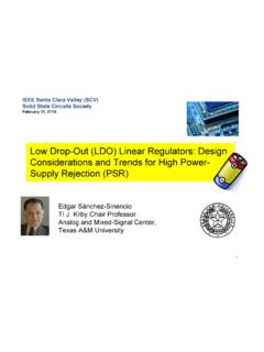
4 Texas Instru-ments recommends that all integrated circuits be handled withappropriate precautions. Failure to observe proper handlingand installation procedures can cause damage can range from subtle performance degradationto complete device failure. Precision integrated circuits may bemore susceptible to damage because very small parametricchanges could cause the device not to meet its (T-1)NOTE: Tabs are electrically connected to the V VOV+VIN VIN+123456E/S77-LeadDDPAK (FA)Surface-MountILIMV VOV+VIN VIN+123456E/S77-LeadStagger-FormedTO-220 (T)ILIMV VOV+VIN VIN+123456 CHARACTERISTICSAt TCASE = +25 C, VS = 30V and E/S pin open, unless otherwise , FPARAMETERCONDITIONMINTYPMAXUNITSOFFSET VOLTAGEI nput Offset VoltageVCM = 0, IO = 0 2 10mVvs TemperatureTA = 40 C to +85 C 30 V/ Cvs power SupplyVS = 4V to 30V30100 V/VINPUT BIAS current (1)Input Bias current (2)VCM = 0V 100 500nAvs TemperatureTA = 40 C to +85 C CInput Offset CurrentVCM = 0V 5 50nANOISEI nput voltage Noise Density, f = 1kHz90nV/ HzCurrent Noise Density, f = 1kHz200fA/ HzINPUT voltage RANGEC ommon-Mode voltage Range.
5 PositiveLinear Operation(V+) 3(V+) Operation(V ) (V ) RejectionVCM = (V ) to (V+) 3V8095dBINPUT IMPEDANCED ifferential107 || 6 || pFCommon-Mode109 || 4 || pFOPEN-LOOP GAINOpen-Loop voltage GainVO = 25V, RL = 1k 9098dBVO = 25V, RL = 8 90dBFREQUENCY RESPONSEGain-Bandwidth ProductRL = 8 1 MHzSlew RateG = 1, 50Vp-p, RL = 8 10V/ sFull- power BandwidthSee Typical CharacteristicskHzSettling Time: = 10, 50V Step15 sTotal Harmonic Distortion + Noise, f = 1kHzRL = 8 , G = +3, power = (3)%OUTPUTV oltage Output, PositiveIO = 3A(V+) (V+) = 3A(V ) + (V ) + = (V+) (V+) = (V ) + (V ) + Continuous current Output: dc 3 Aac3 ArmsLeakage current , Output Disabled, dcSee Typical CharacteristicsOutput current LimitCurrent Limit Range0 to 5 ACurrent Limit EquationILIM = (15000)( )/(13750 + RCL)ACurrent Limit Tolerance(1)RCL = (ILIM = ), 100 250mARL = 8 Capacitive Load DriveSee Typical Characteristics(4)OUTPUT ENABLE /STATUS (E/S) PINS hutdown Input ModeVE/S high (output enabled)E/S Pin Open or Forced high (V ) + LOW (output disabled)E/S Pin Forced Low(V ) + high (output enabled)E/S Pin high 65 AIE/S LOW (output disabled)E/S Pin Low 70 AOutput Disable Time1 sOutput Enable Time3 sThermal Shutdown Status OutputNormal OperationSourcing 20 A(V ) + (V ) + ShutdownSinking 5 A, TJ > 160 C(V ) + (V )
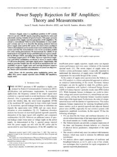
6 + Temperature, Shutdown+160 CReset from Shutdown+140 CPOWER SUPPLYS pecified voltage 30 VOperating voltage Range 4 30 VQuiescent CurrentILIM Connected to V , IO = 0 17 20mAQuiescent current , Shutdown ModeILIM Connected to V , IO = 0 6mATEMPERATURE RANGES pecified Range 40+85 COperating Range 40+125 CStorage Range 55+125 CThermal Resistance, JC7-Lead DDPAK, 7-Lead TO-220f > 50Hz2 C/W7-Lead DDPAK, 7-Lead C/WThermal Resistance, JA7-Lead DDPAK, 7-Lead TO-220No Heat Sink65 C/WNOTES: (1) high -speed test at TJ = +25 C. (2) Positive conventional current flows into the input terminals. (3) See Total Harmonic Distortion+Noise vs Frequency inthe Typical Characteristics section for additional power levels. (4) See Small-Signal Overshoot vs Load Capacitance in the Typical Characteristics CHARACTERISTICSAt TCASE = +25 C, VS = 30V and E/S pin open, unless otherwise 20 Gain (dB)0 45 90 135 180 Phase ( )Frequency (Hz)OPEN-LOOP GAIN AND PHASEvs FREQUENCY GNoLoadRL = 8 RL = 8 No Load0 5 10 15 20 25 30 5 4 3 2 10 current Limit (A) supply voltage (V) current LIMIT vs supply VOLTAGERCL = RCL = RCL = 75 50 250255075100125 160 140 120 100 80 60 40 Input Bias current (nA)Temperature ( C)INPUT BIAS current vs TEMPERATUREVS = 5 VVS = 30V 30 20 100 102030 200 150 100 500 Input Bias current (nA)Common-Mode voltage (V)INPUT BIAS CURRENTvs COMMON-MODE voltage 75 50 250255075100125 20 18 16 14 12 10 8 6 4 Quiescent current (mA)Temperature ( C)QUIESCENT current vs TEMPERATUREVS = 5 VIQVS = 30 VVS = 5 VVS = 30 VIQ Shutdown 75 50 250255075100125 5 4 3 2 10 current Limit (A)Temperature ( C)
7 current LIMIT vs TEMPERATURERCL = RCL = RCL = +ILIM CHARACTERISTICS (Cont.)At TCASE = +25 C, VS = 30V and E/S pin open, unless otherwise rejection (dB)Frequency (Hz)COMMON-MODE rejection vs FREQUENCY 75 50 Product (MHz)Slew Rate (V/ s)Temperature ( C)GAIN-BANDWIDTH PRODUCT ANDSLEW RATE vs TEMPERATURESR+SR GBW1101001k10k100k1M5004003002001000 voltage Noise (nV/ Hz)Frequency (Hz) voltage NOISE DENSITY vs FREQUENCY201001k10k +N (%)Frequency (Hz)TOTAL HARMONIC DISTORTION+NOISEvs FREQUENCYG = +3RL = 8 supply rejection (dB)Frequency (Hz) power - supply REJECTIONvs FREQUENCY+PSRR PSRR 75 50 250255075100 AOL12510095908580 AOL, PSRR (dB)1101051009590 CMRR (dB)Temperature ( C)OPEN-LOOP GAIN, COMMON-MODE rejection ,AND power - supply rejection vs CHARACTERISTICS (Cont.)At TCASE = +25 C, VS = 30V and E/S pin open, unless otherwise 4543210 VSUPPLY VOUT (V)Output current (A)OUTPUT voltage SWING vs OUTPUT current (V+) VO (V ) VO 543210 VSUPPLY VOUT (V)Temperature ( C)OUTPUT voltage SWING vs TEMPERATURE 75 50 250255075100125IO = +3 AIO = 3 AIO = + = voltage (Vp)Frequency (Hz)MAXIMUM OUTPUT voltage SWINGvs FREQUENCYM aximum OutputVoltage WithoutSlew Rate InducedDistortionOFFSET VOLTAGEPRODUCTION DISTRIBUTIONP ercent of Amplifiers (%)Offset voltage (mV) 10 9 8 7 6 5 4 3 2 101234567891020181614121086420 Typical distributionof packaged units.
8 OFFSET voltage DRIFTPRODUCTION DISTRIBUTIONP ercent of Amplifiers (%)Offset voltage Drift ( V/ C)14121086420 Typical productiondistribution ofpackaged units. 0102030405060708090100110120130 40 30 20 100102040301050 5 10 Leakage current (mA)Output voltage (V)OUTPUT LEAKAGE CURRENTvs APPLIED OUTPUT VOLTAGERL = 8 Output DisabledVE/S < (V ) + = RCL = CHARACTERISTICS (Cont.)At TCASE = +25 C, VS = 30V and E/S pin open, unless otherwise 12k 14k 16k 18k 20k50403020100 Overshoot (%)Load Capacitance (pF)SMALL-SIGNAL OVERSHOOTvs LOAD CAPACITANCEG = 1G = +1 SMALL-SIGNAL STEP RESPONSEG = 3, CL = 1000pF100mV/div2 s/divLARGE-SIGNAL STEP RESPONSEG = 3, CL = 1000pF, RL = 8 10V/div5 s/divSMALL-SIGNAL STEP RESPONSEG = 1, CL = 1000pF50mV/div2 INFORMATIONF igure 1 shows the OPA548 connected as a basic noninvertingamplifier. The OPA548 can be used in virtually any op terminals should be bypassed with low seriesimpedance capacitors.
9 The technique shown in Figure 7,using a ceramic and tantalum type in parallel is recom-mended. In addition, we recommend a F capacitorbetween V+ and V as close to the OPA548 as wiring should have low series the OPA548, the simplest method for adjusting thecurrent limit uses a resistor or potentiometer connectedbetween the ILIM pin and V according to the Equation 1:RICLLIM=()()15000 4 7513750. The low-level control signal (0 A to 330 A) also allows thecurrent limit to be digitally Figure 3 for a simplified schematic of the internalcircuitry used to set the current limit. Leaving the ILIM pinopen programs the output current to zero, while connectingILIM directly to V programs the maximum output current limit,typically OPERATING AREAS tress on the output transistors is determined both by theoutput current and by the output voltage across the conduct-ing output transistor, VS VO.
10 The power dissipated by theoutput transistor is equal to the product of the output currentand the voltage across the conducting transistor, VS Safe Operating Area (SOA curve, Figure 2) shows thepermissible range of voltage and 1. Basic Circuit SUPPLIESThe OPA548 operates from single (+8V to +60V) or dual( 4V to 30V) supplies with excellent performance. Mostbehavior remains unchanged throughout the full operatingvoltage range. Parameters which vary significantly with oper-ating voltage are shown in the typical characteristic applications do not require equal positive and negativeoutput voltage swing. power - supply voltages do not need tobe equal. The OPA548 can operate with as little as 8 Vbetween the supplies and with up to 60V between thesupplies. For example, the positive supply could be set to55V with the negative supply at 5V, or current LIMITThe OPA548 features an accurate, user-selected currentlimit.