Transcription of HV9910C - Microchip Technology
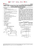
1 HV9910C . Universal High-Brightness LED Driver Features Description Switch mode controller for single switch LED drivers HV9910C is an open-loop, current -mode control, LED. Enhanced drop-in replacement to the HV9910B driver IC. This IC can be programmed to operate in either a constant frequency or constant off-time mode. Open loop peak current controller It includes a 15 450V linear regulator which allows it Internal 15 to 450V linear regulator to work with a wide range of input voltages without the Constant frequency or constant off-time operation need for an external low voltage supply. HV9910C . Linear and PWM dimming capability includes a TTL-compatible, PWM-dimming input that Requires few external components for operation can accept an external control signal with a duty ratio of 0 100% and a frequency of up to a few kilohertz.
2 It Over-temperature protection also includes a 0 250mV linear-dimming input which can be used for linear dimming of the LED current . Applications Unlike the HV9910B, the HV9910C is equipped with DC/DC or AC/DC LED driver applications built-in thermal-shutdown protection. RGB back-lighting LED driver HV9910C is ideally suited for buck LED drivers. Since Back lighting of flat panel displays the HV9910C operates in open-loop current mode con- trol, the controller achieves good output current regula- General purpose constant current source tion without the need for any loop compensation. Also, Signage and decorative LED lighting being an open-loop controller, PWM-dimming Chargers response is limited only by the rate of rise of the induc- tor current , enabling a very fast rise and fall times of the LED current .
3 HV9910C requires only three external components (apart from the power stage) to produce a controlled LED current . This makes HV9910C an ideal solution for low-cost LED drivers. 2014 Microchip Technology Inc. DS20005323A-page 1. HV9910C . TO OUR VALUED CUSTOMERS. It is our intention to provide our valued customers with the best documentation possible to ensure successful use of your Microchip products. To this end, we will continue to improve our publications to better suit your needs. Our publications will be refined and enhanced as new volumes and updates are introduced. If you have any questions or comments regarding this publication, please contact the Marketing Communications Department via E-mail at We welcome your feedback. Most current Data Sheet To obtain the most up-to-date version of this data sheet, please register at our Worldwide Web site at: You can determine the version of a data sheet by examining its literature number found on the bottom outside corner of any page.
4 The last character of the literature number is the version number, ( , DS30000000A is version A of document DS30000000). Errata An errata sheet, describing minor operational differences from the data sheet and recommended workarounds, may exist for current devices. As device/documentation issues become known to us, we will publish an errata sheet. The errata will specify the revision of silicon and revision of document to which it applies. To determine if an errata sheet exists for a particular device, please check with one of the following: Microchip 's Worldwide Web site; Your local Microchip sales office (see last page). When contacting a sales office, please specify which device, revision of silicon and data sheet (include literature number) you are using. Customer Notification System Register on our web site at to receive the most current information on all of our products.
5 DS20005323A-page 2 2014 Microchip Technology Inc. HV9910C . Pin Diagram VIN 1 16 NC. NC 2 15 NC. NC 3 14 RT. CS 4 13 LD. VIN 1 8 RT GND 5 12 VDD. CS 2 7 LD NC 6 11 NC. GND 3 6 VDD NC 7 10 NC. GATE 4 5 PWMD GATE 8 9 PWMD. 8-Lead SOIC 16-Lead SOIC. Typical Application Circuit CIN. CO. D1. CDD L1. VIN. VDD. HV9910C . LD. GATE Q1. PWMD CS. RT GND. ROSC RCS. 2014 Microchip Technology Inc. DS20005323A-page 3. HV9910C . ELECTRICAL. CHARACTERISTICS. ABSOLUTE MAXIMUM RATINGS. VIN to GND .. to +470V. VDD to CS, LD, PWMD, to (VDD + ). Junction temperature ..-40 C to +125 C. Storage temperature ..-65 C to +150 C. Continuous power dissipation (TA = +25 C). 8-lead SOIC ..650 mW. 16-lead SOIC ..1300 mW. 8-lead SOIC with heat slug ..1300 mW. Note: Stresses above those listed under Absolute Maximum Ratings may cause permanent damage to the device.
6 This is a stress rating only and functional operation of the device at those or any other conditions, above those indicated in the operational listings of this specification, is not implied. Expo- sure to maximum rating conditions for extended periods may affect device reliability. ELECTRICAL SPECIFICATIONS. TABLE 1-1: ELECTRICAL CHARACTERISTICS (SHEET 1 OF 2)1. Symbol Parameter Note Min Typ Max Units Conditions Input Input DC supply voltage 3. VINDC 15 - 450 V DC input voltage range2. Pin PWMD to VDD, no capaci- IIN(MAX) Supply current - - mA. tance at GATE. Shut-down mode supply IINSD - - mA Pin PWMD to GND. current Internal Regulator VIN = 15V, IDD(ext) = 0, VDD Internally regulated voltage - V PWMD = VDD, 500pF at GATE;. ROSC = 249k . VIN = 15 - 450V, IDD(ext) = 0, VDD, line Line regulation of VDD - 0 - V PWMD = VDD, 500pF at GATE.
7 ROSC = 249k . IDD(ext) = 0 - , VDD, load Load regulation of VDD - 0 - V PWMD = VDD, 500pF at GATE;. ROSC = 249k . VDD under voltage lockout 3. UVLO V VDD rising threshold VDD under voltage lockout UVLO - - 500 - mV VDD falling hysteresis 4. IIN(MAX) Maximum regulator current - - mA VDD = UVLO - UVLO. PWM Dimming 3. VEN(lo) PWMD input low voltage - - V VIN = 15 - 450V. VEN(hi) 3. PWMD input high voltage - - V VIN = 15 - 450V. Internal pull-down resis- REN - 50 100 150 k VPWMD = tance at PWMD. DS20005323A-page 4 2014 Microchip Technology Inc. HV9910C . TABLE 1-1: ELECTRICAL CHARACTERISTICS (CONTINUED) (SHEET 2 OF 2)1. Symbol Parameter Note Min Typ Max Units Conditions current Sense Comparator current sense pull-in thresh- VCS - 225 250 275 mV -40 C < TA < +125 C. old voltage Offset voltage for LD com- 3.
8 VOFFSET -12 - +12 mV. parator 0 < TA < +85 C, VLD = VDD, - 150 215 280 VCS = VCS,TH + 50mV after current sense blanking TBLANK. TBLANK ns interval -40 < TA < +125 C, VLD = VDD, - 145 215 315 VCS = VCS,TH + 50mV after TBLANK. VIN = 15V, VLD = , tDELAY Delay to output - - 80 150 ns VCS = 0 to after tBLANK. Oscillator - 20 25 30 ROSC = . fOSC Oscillator frequency kHz - 80 100 120 ROSC = 249k . Gate Driver Maximum GATE sourcing ISOURCE - - - A VGATE = 0V. current Maximum GATE sinking cur- ISINK - - - A VGATE = VDD. rent 4. tRISE GATE output rise time - 30 50 ns CGATE = 500pF. tFALL 4. GATE output fall time - 30 50 ns CGATE = 500pF. Over-Temperature Protection TSD Shut-down temperature - 128 - 150 C. TSD Hysteresis - 10 - 30 C. ISD TSD-mode VIN current - - - 350 A. 1 Specifications are TA = 25 C, VIN = 15V unless otherwise noted.
9 2 Also limited by package-power dissipation limit; Whichever is lower. 3 Applies over the full operating ambient temperature range of -40 C < TA < +125 C. 4 For design guidance only. TABLE 1-2: THERMAL RESISTANCE. Package ja 8-Lead SOIC 101 C/W. 16-Lead SOIC 83 C/W. 8-Lead SOIC (with heat slug) 84 C/W. 2014 Microchip Technology Inc. DS20005323A-page 5. HV9910C . PIN DESCRIPTION. The descriptions of the pins are listed in Table 2-1. TABLE 2-1: PIN DESCRIPTION. Pin #. Function Description 8-Lead SOIC 16-Lead SOIC. 1 1 VIN Input of an 15 - 450V linear regulator. 2 4 CS current sense pin used to sense the FET current by means of an external sense resistor. When this pin exceeds the lower of either the internal 250mV or the voltage at the LD pin, the GATE output goes low. 3 5 GND Ground return for all internal circuitry.
10 Must be electrically con- nected to the power ground. 4 8 GATE Output GATE driver for an external N-channel power MOSFET. 5 9 PWMD TTL-compatible, PWM-dimming input of the IC. When this pin is pulled to GND or left open, the GATE driver is turned off. When the pin is pulled high, the GATE driver operates normally. 6 12 VDD Power supply pin for all internal circuits. It must be bypassed with a low ESR capacitor to GND ( F). 7 13 LD Linear-dimming input and sets the current sense threshold as long as the voltage at the pin is less than 250mV (typ). 8 14 RT Sets the oscillator frequency. When a resistor is connected between RT and GND, the HV9910C operates in constant fre- quency mode. When the resistor is connected between RT and GATE, the IC operates in constant off-time mode. - 2, 3, 6, 7, 10, NC No connection 11, 15, 16.