Transcription of Infrared Transceiver Module (SIR, 115.2 kbit/s) for …
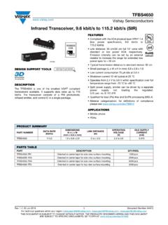
1 Semiconductors Rev. , 29-Jun-20181 Document Number: 81288 For technical questions within your region: DOCUMENT IS SUBJECT TO CHANGE WITHOUT NOTICE. THE PRODUCTS DESCRIBED HEREIN AND THIS DOCUMENTARE SUBJECT TO SPECIFIC DISCLAIMERS, SET FORTH AT Transceiver Module (SIR, kbit/s) for IrDA ApplicationsDESIGN SUPPORT TOOLSDESCRIPTIONThe TFDU4101 Transceiver is an Infrared Transceiver Module compliant to the latest IrDA physical layer standard for fast Infrared data communication, supporting IrDA speeds up to kbit/s (SIR), and carrier based remote control modes. Integrated within the Transceiver Module are a photo pin diode, an Infrared emitter (IRED), and a low-power control IC to provide a total front-end solution in a single package.
2 This device covers the full IrDA range of more than 1 m using the internal intensity control. With one external current control resistor the current can be adjusted for shorter ranges saving operating current operating in IrDA low power mode. This vishay SIR Transceiver is using the lead frame receiver output pulse duration is independent of the optical input pulse duration and recovers always a fixed pulse duration optimum for compatibility to standard Endecs and interfaces. TFDU4101 has a tristate output and is floating in shutdown mode with a weak Operates from V to V within specification over full temperature range from -30 C to +85 C Split power supply, transmitter and receiver can be operated from two power supplies with relaxed requirements saving costs, US - patent no.
3 6,157,476 Low power consumption (< mA supply current in receive mode, no signal) Power shutdown mode (< 4 A shutdown current in full temperature range, up to 85 C, < 10 nA at 25 C) Surface-mount package (L x W x H in mm): 4 High efficiency emitter Low profile (universal) package capable of surface mount soldering to side and top view orientation Directly Interfaces with various super I/O and controller devices as e. g. TOIM4232 Tri-state-receiver output, floating in shut down with a weak pull-up Qualified for lead (Pb)-free and Sn/Pb processing (MSL4) Material categorization.
4 For definitions of compliance please see Printers, fax machines, photocopiers, screen projectors Internet TV boxes, video conferencing systems Medical data collection Diagnostic systems Notebook computers, desktop PCs, palmtop computers (Win CE, Palm PC), PDAs Internet TV boxes, video conferencing systems External Infrared adapters (dongles) Data loggers GPS Kiosks, POS, point and pay devices Industrial applications20110click logo to get startedAvailableModelsPRODUCT SUMMARYPART NUMBERDATA RATE( kbit/s) DIMENSIONSH x L x W(mm x mm x mm)LINK DISTANCE(m)OPERATING VOLTAGE(V)IDLE SUPPLY CURRENT(mA) x x to to TABLEPARTDESCRIPTIONQTY/REELTFDU4101-TR3 Oriented in carrier tape for side view surface mounting1000 pcsTFDU4101-TT3 Oriented in carrier tape for top view surface mounting1000 Semiconductors Rev.
5 , 29-Jun-20182 Document Number: 81288 For technical questions within your region: DOCUMENT IS SUBJECT TO CHANGE WITHOUT NOTICE. THE PRODUCTS DESCRIBED HEREIN AND THIS DOCUMENTARE SUBJECT TO SPECIFIC DISCLAIMERS, SET FORTH AT BLOCK DIAGRAMPIN DESCRIPTIONPIN NUMBER SYMBOLDESCRIPTIONI/OACTIVE1 VCC2 IRED anodeIRED anode to be externally connected to VCC2. An external resistor is only necessary for controlling the IRED current when a current reduction below 300 mA is intended to operate in IrDA low power pin is allowed to be supplied from an uncontrolled power supply separated from the controlled VCC1 - supply.
6 2 IRED cathodeIRED cathode, internally connected to driver transistor3 TXDThis Schmitt-Trigger input is used to transmit serial data when SD is low. An on-chip protection circuit disables the LED driver if the TXD pin is asserted for longer than 50 s (max. 300 s). IHigh4 RXDR eceived data output, push-pull CMOS driver output capable of driving standard CMOS or TTL loads. During transmission the RXD output is active (echo-on). No external pull-up or pull-down resistor is required. Floating with a weak pull-up of 500 k (typ.) in shutdown voltage7 NCNo internal connectionI8 GNDG roundControlleddriverTri-statedriverGNDT XDRXDVCC2 VCC1 SDIRED Semiconductors Rev.
7 , 29-Jun-20183 Document Number: 81288 For technical questions within your region: DOCUMENT IS SUBJECT TO CHANGE WITHOUT NOTICE. THE PRODUCTS DESCRIBED HEREIN AND THIS DOCUMENTARE SUBJECT TO SPECIFIC DISCLAIMERS, SET FORTH AT Weight 200 mg Note Reference point pin, GND unless otherwise noted. Typical values are for DESIGN AID ONLY, not guaranteed nor subject to production testingNote vishay transceivers operating inside the absolute maximum ratings are classified as eye safe according the above tableABSOLUTE MAXIMUM RATINGSPARAMETERTEST voltage range, V < VCC2 < 6 voltage range, V < VCC1 < 6 at V < VCC1 < 6 + at all inputs and outputsVin > VCC1 is currentsFor all pins, except IRED anode pin--10mAOutput sinking current--25mAPower dissipationSee derating curvePD--250mWJunction temperatureTJ--125 CAmbient temperature range (operating)
8 Tamb-30-+85 CStorage temperature rangeTstg-30-+85 CSoldering temperatureSee Recommended Solder Profile --260 CAverage output current, pin 1 IIRED (DC)--80mARepetitive pulse output current, pin 1 to pin 2< 90 s, ton < 20 %IIRED (RP)--400mAEYE SAFETY INFORMATIONSTANDARDCLASSIFICATIONIEC/EN 60825-1 (2007-03), DIN EN 60825-1 (2008-05) SAFETY OF LASER PRODUCTS - Part 1: equipment classification and requirements , simplified methodClass 1 IEC 62471 (2006), CIE S009 (2002) Photobiological Safety of Lamps and Lamp Systems ExemptDIRECTIVE 2006/25/EC OF THE EUROPEAN PARLIAMENT AND OF THE COUNCIL of 5th April 2006 on the minimum health and safety requirements regarding the exposure of workers to risks arising from physical agents (artificial optical radiation) (19th individual directive within the meaning of article 16(1) of directive 89/391/EEC)Exempt U Option Baby Face (universal) Semiconductors Rev.
9 , 29-Jun-20184 Document Number: 81288 For technical questions within your region: DOCUMENT IS SUBJECT TO CHANGE WITHOUT NOTICE. THE PRODUCTS DESCRIBED HEREIN AND THIS DOCUMENTARE SUBJECT TO SPECIFIC DISCLAIMERS, SET FORTH AT Typical values are for DESIGN AID ONLY, not guaranteed nor subject to production testing(1)Standard illuminant A(2)The typical threshold level is x VCC1. It is recommended to use the specified values to avoid increased operating currentELECTRICAL CHARACTERISTICS (Tamb = 25 C, VCC1 = VCC2 = V to V unless otherwise noted)PARAMETERTEST supply currentSD = low, Ee = 1 klx (1),Tamb = -25 C to +85 CVCC1 = VCC2 = V to VICC14090130 ADynamic supply currentSD = low, Ee = 1 klx (1)
10 ,Tamb = 25 CVCC1 = VCC2 = V to VICC14075- AAverage dynamic supply current, transmittingIIRED = 300 mA,25 % duty supply currentSD = high, T = 25 C, Ee = 0 klxno signal, no resistive ASD = high, T = 70 Cno signal, no resistive loadISD--1 ASD = high, T = 85 Cno signal, no resistive loadISD--1 AOperating temperature rangeTA-30-+85 COutput voltage low, RXDC load = 15 x VCC1 VOutput voltage high, RXDIOH = -500 A, CLoad = 15 x VCC1-VCC1 + = -250 A, CLoad = 15 x VCC1-VCC1 + to VCC1 impedanceRRXD400500600k Input voltage low (TXD, SD) voltage high (TXD, SD) V Vlogic V (2) x VCC1-6 VVlogic > V (2)VIHVCC1 - leakage current (TXD, SD)Vin = x VCC1 IICH-2-+2 AControlled pull down current 0 < Vin < VCC1 Vin > VCC1SD, TXD = 0 or 1 IIrTX-10+1501 A AInput capacitance (TXD, SD) Semiconductors Rev.
